Intel D945GCNL Product Specification - Page 7

Regulatory Compliance and Battery Disposal Information, s, Tables - audio

Page 7 highlights

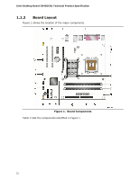
Contents 5 Regulatory Compliance and Battery Disposal Information 5.1 Regulatory Compliance 77 5.1.1 Safety Standards 77 5.1.2 European Union Declaration of Conformity Statement 78 5.1.3 Product Ecology Statements 79 5.1.4 EMC Regulations 83 5.1.5 Product Certification Markings (Board Level 85 5.2 Battery Disposal Information 86 Figures 1. Board Components 12 2. Block Diagram 14 3. Back Panel Audio Connector Options 25 4. LAN Connector LED Locations 27 5. Thermal Sensors and Fan Headers 29 6. Location of the Standby Power Indicator LED 35 7. Detailed System Memory Address Map 38 8. Back Panel Connectors 45 9. Component-side Connectors and Headers 46 10. Connection Diagram for Front Panel Header 51 11. Connection Diagram for Front Panel USB Headers 53 12. Location of the Jumper Block 54 13. Board Dimensions 56 14. Localized High Temperature Zones 60 Tables 1. Feature Summary 10 2. Board Components Shown in Figure 1 13 3. Supported Memory Configurations 16 4. LAN Connector LED States 27 5. Effects of Pressing the Power Switch 30 6. Power States and Targeted System Power 31 7. Wake-up Devices and Events 32 8. System Memory Map 39 9. DMA Channels 39 10. I/O Map 40 11. PCI Configuration Space Map 41 12. Interrupts 42 13. PCI Interrupt Routing Map 43 14. Component-side Connectors and Headers Shown in Figure 9 47 15. Front Panel Audio Header 48 16. Chassis Intrusion Header 48 17. Serial ATA Connectors 48 18. Processor Fan Header 48 19. Front and Rear Chassis Fan Headers 48 vii

  • 1
  • 2
  • 3
  • 4
  • 5
  • 6
  • 7
  • 8
  • 9
  • 10
  • 11
  • 12
  • 13
  • 14
  • 15
  • 16
  • 17
  • 18
  • 19
  • 20
  • 21
  • 22
  • 23
  • 24
  • 25
  • 26
  • 27
  • 28
  • 29
  • 30
  • 31
  • 32
  • 33
  • 34
  • 35
  • 36
  • 37
  • 38
  • 39
  • 40
  • 41
  • 42
  • 43
  • 44
  • 45
  • 46
  • 47
  • 48
  • 49
  • 50
  • 51
  • 52
  • 53
  • 54
  • 55
  • 56
  • 57
  • 58
  • 59
  • 60
  • 61
  • 62
  • 63
  • 64
  • 65
  • 66
  • 67
  • 68
  • 69
  • 70
  • 71
  • 72
  • 73
  • 74
  • 75
  • 76
  • 77
  • 78
  • 79
  • 80
  • 81
  • 82
  • 83
  • 84
  • 85
  • 86
  • 87
  • 88
  • 89
  • 90

Contents
vii
5
Regulatory Compliance and Battery Disposal Information
5.1
Regulatory Compliance
.....................................................................
77
5.1.1
Safety Standards
..................................................................
77
5.1.2
European Union Declaration of Conformity Statement
................
78
5.1.3
Product Ecology Statements
...................................................
79
5.1.4
EMC Regulations
..................................................................
83
5.1.5
Product Certification Markings (Board Level)
.............................
85
5.2
Battery Disposal Information
.............................................................
86
Figures
1.
Board Components
..........................................................................
12
2.
Block Diagram
................................................................................
14
3.
Back Panel Audio Connector Options
..................................................
25
4.
LAN Connector LED Locations
............................................................
27
5.
Thermal Sensors and Fan Headers
.....................................................
29
6.
Location of the Standby Power Indicator LED
.......................................
35
7.
Detailed System Memory Address Map
...............................................
38
8.
Back Panel Connectors
.....................................................................
45
9.
Component-side Connectors and Headers
...........................................
46
10. Connection Diagram for Front Panel Header
........................................
51
11. Connection Diagram for Front Panel USB Headers
................................
53
12. Location of the Jumper Block
.............................................................
54
13. Board Dimensions
...........................................................................
56
14. Localized High Temperature Zones
.....................................................
60
Tables
1.
Feature Summary
............................................................................
10
2.
Board Components Shown in Figure 1
................................................
13
3.
Supported Memory Configurations
.....................................................
16
4.
LAN Connector LED States
................................................................
27
5.
Effects of Pressing the Power Switch
..................................................
30
6.
Power States and Targeted System Power
...........................................
31
7.
Wake-up Devices and Events
............................................................
32
8.
System Memory Map
.......................................................................
39
9.
DMA Channels
.................................................................................
39
10.
I/O Map
.........................................................................................
40
11.
PCI Configuration Space Map
............................................................
41
12.
Interrupts
......................................................................................
42
13.
PCI Interrupt Routing Map
................................................................
43
14.
Component-side Connectors and Headers Shown in Figure 9
.................
47
15.
Front Panel Audio Header
.................................................................
48
16.
Chassis Intrusion Header
..................................................................
48
17.
Serial ATA Connectors
......................................................................
48
18.
Processor Fan Header
......................................................................
48
19.
Front and Rear Chassis Fan Headers
..................................................
48