Intel DB43LD Product Specification - Page 7

Regulatory Compliance and Battery Disposal Information, s, Tables - front panel header details

Page 7 highlights

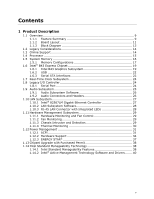
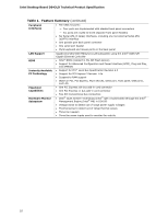
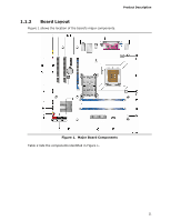
Contents 5 Regulatory Compliance and Battery Disposal Information 5.1 Regulatory Compliance 81 5.1.1 Safety Standards 81 5.1.2 European Union Declaration of Conformity Statement 82 5.1.3 Product Ecology Statements 83 5.1.4 EMC Regulations 87 5.1.5 Product Certification Markings (Board Level 88 5.2 Battery Disposal Information 89 Figures 1. Major Board Components 11 2. Block Diagram 13 3. Memory Channel and DIMM Configuration 18 4. Back Panel Audio Connector Options 26 5. LAN Connector LED Locations 28 6. Thermal Sensors and Fan Headers 30 7. Location of the Standby Power Indicator LED 37 8. Detailed System Memory Address Map 42 9. Back Panel Connectors 45 10. Component-side Connectors and Headers 46 11. Connection Diagram for Front Panel Header 51 12. Connection Diagram for Front Panel USB Headers 54 13. Location of the BIOS Configuration Jumper Block 55 14. Board Dimensions 57 15. Localized High Temperature Zones 60 Tables 1. Feature Summary 9 2. Board Components Shown in Figure 1 12 3. Supported Memory Configurations 16 4. DVI Port Status Conditions 21 5. Audio Jack Retasking Support 25 6. LAN Connector LED States 28 7. Effects of Pressing the Power Switch 31 8. Power States and Targeted System Power 32 9. Wake-up Devices and Events 33 10. System Memory Map 43 11. Component-side Connectors and Headers Shown in Figure 10 47 12. Front Panel Audio Header for HD Audio 48 13. Front Panel Audio Header for AC '97 Audio 48 14. Serial ATA Connectors 48 15. Serial Port Header 48 16. Chassis Intrusion Header 49 17. Front, Rear, and Processor (4-Pin) Fan Header 49 18. Processor Core Power Connector 50 vii

  • 1
  • 2
  • 3
  • 4
  • 5
  • 6
  • 7
  • 8
  • 9
  • 10
  • 11
  • 12
  • 13
  • 14
  • 15
  • 16
  • 17
  • 18
  • 19
  • 20
  • 21
  • 22
  • 23
  • 24
  • 25
  • 26
  • 27
  • 28
  • 29
  • 30
  • 31
  • 32
  • 33
  • 34
  • 35
  • 36
  • 37
  • 38
  • 39
  • 40
  • 41
  • 42
  • 43
  • 44
  • 45
  • 46
  • 47
  • 48
  • 49
  • 50
  • 51
  • 52
  • 53
  • 54
  • 55
  • 56
  • 57
  • 58
  • 59
  • 60
  • 61
  • 62
  • 63
  • 64
  • 65
  • 66
  • 67
  • 68
  • 69
  • 70
  • 71
  • 72
  • 73
  • 74
  • 75
  • 76
  • 77
  • 78
  • 79
  • 80
  • 81
  • 82
  • 83
  • 84
  • 85
  • 86
  • 87
  • 88
  • 89
  • 90
  • 91
  • 92

Contents
vii
5
Regulatory Compliance and Battery Disposal Information
5.1
Regulatory Compliance
.....................................................................
81
5.1.1
Safety Standards
..................................................................
81
5.1.2
European Union Declaration of Conformity Statement
................
82
5.1.3
Product Ecology Statements
...................................................
83
5.1.4
EMC Regulations
..................................................................
87
5.1.5
Product Certification Markings (Board Level)
.............................
88
5.2
Battery Disposal Information
.............................................................
89
Figures
1.
Major Board Components
..................................................................
11
2.
Block Diagram
................................................................................
13
3.
Memory Channel and DIMM Configuration
...........................................
18
4.
Back Panel Audio Connector Options
..................................................
26
5.
LAN Connector LED Locations
............................................................
28
6.
Thermal Sensors and Fan Headers
.....................................................
30
7.
Location of the Standby Power Indicator LED
.......................................
37
8.
Detailed System Memory Address Map
...............................................
42
9.
Back Panel Connectors
.....................................................................
45
10. Component-side Connectors and Headers
...........................................
46
11. Connection Diagram for Front Panel Header
........................................
51
12. Connection Diagram for Front Panel USB Headers
................................
54
13. Location of the BIOS Configuration Jumper Block
.................................
55
14. Board Dimensions
...........................................................................
57
15. Localized High Temperature Zones
.....................................................
60
Tables
1.
Feature Summary
..............................................................................
9
2.
Board Components Shown in Figure 1
................................................
12
3.
Supported Memory Configurations
.....................................................
16
4.
DVI Port Status Conditions
................................................................
21
5.
Audio Jack Retasking Support
...........................................................
25
6.
LAN Connector LED States
................................................................
28
7.
Effects of Pressing the Power Switch
..................................................
31
8.
Power States and Targeted System Power
...........................................
32
9.
Wake-up Devices and Events
............................................................
33
10. System Memory Map
.......................................................................
43
11. Component-side Connectors and Headers Shown in Figure 10
................
47
12. Front Panel Audio Header for HD Audio
...............................................
48
13. Front Panel Audio Header for AC ’97 Audio
..........................................
48
14. Serial ATA Connectors
......................................................................
48
15. Serial Port Header
...........................................................................
48
16. Chassis Intrusion Header
..................................................................
49
17. Front, Rear, and Processor (4-Pin) Fan Header
....................................
49
18. Processor Core Power Connector
........................................................
50