Intel DP55SB Product Guide - Page 54
Chassis Intrusion Header, S/PDIF Header, Table 11. Chassis Intrusion Header Signal Names
 |
UPC - 735858206006
View all Intel DP55SB manuals
Add to My Manuals
Save this manual to your list of manuals |
Page 54 highlights
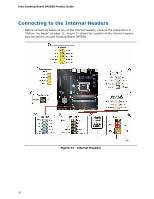
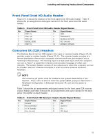
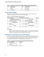
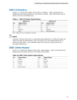
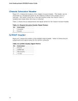
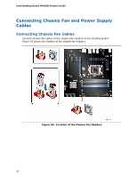
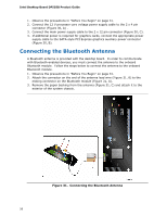
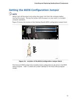
Intel Desktop Board DP55SB Product Guide Chassis Intrusion Header Figure 27, H shows the location of the chassis intrusion header. This header can be connected to a mechanical switch on the chassis to detect if the chassis cover is removed. This switch should be in the open position when the chassis cover is installed and closed when the cover is removed. Table 11 shows the pin assignments and signal names for the chassis intrusion header. Table 11. Chassis Intrusion Header Signal Names Pin Description 1 Intruder# 2 Ground S/PDIF Header Figure 27, I shows the location of the S/PDIF output header. Table 12 shows the pin assignments and signal names for the S/PDIF connector. Table 12. S/PDIF Header Signal Names Pin Description 1 Ground 2 S/PDIF Out 3 Key (no pin) 4 +5 VDC 54
-
 1
1 -
2
-
3
-
4
-
5
-
6
-
7
-
8
-
9
-
10
-
11
-
12
-
13
-
14
-
15
-
16
-
17
-
18
-
19
-
20
-
21
-
22
-
23
-
24
-
25
-
26
-
27
-
28
-
29
-
30
-
31
-
32
-
33
-
34
-
35
-
36
-
37
-
38
-
39
-
40
-
41
-
42
-
43
-
44
-
45
-
46
-
47
-
48
-
 49
49 -
 50
50 -
 51
51 -
 52
52 -
 53
53 -
 54
54 -
 55
55 -
 56
56 -
 57
57 -
 58
58 -
 59
59 -
60
-
61
-
62
-
63
-
64
-
65
-
66
-
67
-
68
-
69
-
70
-
71
-
72
-
73
-
74
-
75
-
76
-
77
-
78
-
79
-
80
-
81
-
82
-
83
-
84
-
85
-
86
-
87
-
88
-
89
-
90
-
91
-
92
 |
 |