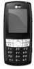
LG KG200 Service Manual - Page 61
Memory, PIN NAMES
 |
View all LG KG200 manuals
Add to My Manuals
Save this manual to your list of manuals |
Page 61 highlights
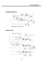
5. Circuit Diagrams Memory PIN NAMES A0 to A22 DQ0 to DQ15 I/O1 to I/O8 CE1ps, CE2ps CEf CEn OE WE REn WEn LB , UB CLE ALE WP/ACC WPn RESET RY/BYf RY/BYn VCCps VCCf VCCn VSS NC Address inputs for Pseudo SRAM & Nor Flash Memory Data inputs / outputs for Pseudo SRAM & Nor Flash Memory Data inputs / outputs for Nand E2PROM Chip enable inputs for Pseudo SRAM Chip enable input for Nor Flash Memory Chip enable input for Nand E2PROM Output enable input for Pseudo SRAM & Nor Flash Memory Write enable input for Pseudo SRAM & Nor Flash Memory Read enable input for Nand E2PROM Write enable input for Nand E2PROM Data vyte control inputs for Pseudo SRAM Command latch enable input for Nand E2PROM Address latch enable input for Nand E2PROM Write protect / program acceleration input for Nor Flash Memory Write protect input for Nand E2PROM Hardware reset input for Nor Flash Memory Ready / Busy output for Nor Flash Memory Ready / Busy output for Nand E2PROM Power supply for Pseudo SRAM Power supply for Nor Flash Memory Power supply for Nand E2PROM Ground Not connected - 62 -
-
 1
1 -
2
-
3
-
4
-
5
-
6
-
7
-
8
-
9
-
10
-
11
-
12
-
13
-
14
-
15
-
16
-
17
-
18
-
19
-
20
-
21
-
22
-
23
-
24
-
25
-
26
-
27
-
28
-
29
-
30
-
31
-
32
-
33
-
34
-
35
-
36
-
37
-
38
-
39
-
40
-
41
-
42
-
43
-
44
-
45
-
46
-
47
-
48
-
49
-
50
-
51
-
52
-
53
-
54
-
55
-
 56
56 -
 57
57 -
 58
58 -
 59
59 -
 60
60 -
 61
61 -
 62
62 -
 63
63 -
 64
64 -
 65
65 -
 66
66 -
67
-
68
-
69
-
70
-
71
-
72
-
73
-
74
-
75
-
76
-
77
-
78
-
79
 |
 |
