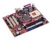
MSI KM4M-V User Guide - Page 14
Serial ATA HDD Connectors: SATA1/SATA2 for KM400/KM400A, FSB Clock Jumper: SW1/SW2, Clear CMOS
 |
UPC - 816909005301
View all MSI KM4M-V manuals
Add to My Manuals
Save this manual to your list of manuals |
Page 14 highlights
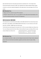
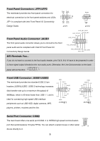
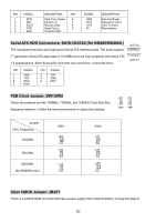
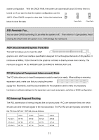
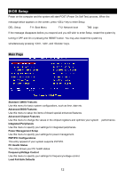
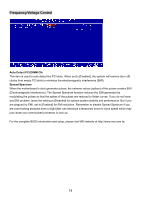
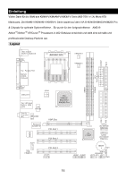
PIN SIGNAL 1 DCD 2 SIN 3 SOUT 4 DTR 5 GND DESCRIPTION PIN Data Carry Detect 6 Serial In or 7 Receive Data 8 Serial Out or 9 Transmit Data SIGNAL DSR RTS CTS RI DESCRIPTION Data Set Ready Request To Send Clear To Send Ring Indicate Serial ATA HDD Connectors: SATA1/SATA2 (for KM400/KM400A ) The mainboard provides dual high-speed Serial ATA interface ports. The ports support 1st generation Serial ATA data rates of 150 MB/s and are fully compliant with Serial ATA 1.0 specifications. Each Serial ATA connector can connect to 1 hard disk drive. SATA2 7 1 SATA1 PIN SIGNAL 1 GND 3 TXN 5 RXN 7 GND PIN SIGNAL 2 TXP 4 GND 6 RXP FSB Clock Jumper: SW1/SW2 These two jumpers provide 100MHz, 133MHz, and 166MHz Front Side Bus frequency selection. Follow the instructions below to adjust the jumpers. 3 3 1 1 SW1 SW2 Jumper CPU Frequency 133 MHz 166 MHz 200 MHz (for KM400A only) SW1 3 1 3 1 3 1 SW2 3 1 3 1 3 1 Clear CMOS Jumper: JBAT1 There is a CMOS RAM on board that has a power supply from external battery to keep the data of 10
-
 1
1 -
2
-
3
-
4
-
5
-
6
-
7
-
8
-
 9
9 -
 10
10 -
 11
11 -
 12
12 -
 13
13 -
 14
14 -
 15
15 -
 16
16 -
 17
17 -
 18
18 -
 19
19 -
20
-
21
-
22
-
23
-
24
-
25
-
26
-
27
-
28
-
29
-
30
-
31
-
32
-
33
-
34
-
35
-
36
-
37
-
38
-
39
-
40
-
41
-
42
-
43
-
44
-
45
-
46
-
47
-
48
-
49
-
50
-
51
-
52
-
53
-
54
-
55
-
56
-
57
-
58
-
59
-
60
-
61
-
62
-
63
-
64
-
65
-
66
-
67
-
68
-
69
-
70
-
71
-
72
-
73
-
74
-
75
-
76
-
77
-
78
-
79
-
80
-
81
-
82
-
83
-
84
-
85
-
86
-
87
-
88
-
89
-
90
-
91
-
92
-
93
-
94
-
95
-
96
-
97
-
98
-
99
-
100
-
101
-
102
 |
 |
