MSI KT880 User Guide - Page 45
Advanced Chipset Features, Con DRAM Timing by SPD, SDRAM CAS# Latency, SDRAM Bank Interleave
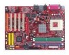 |
UPC - 816909006063
View all MSI KT880 manuals
Add to My Manuals
Save this manual to your list of manuals |
Page 45 highlights
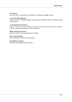
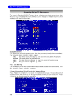
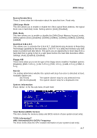
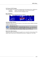
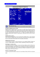
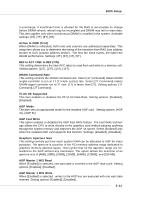
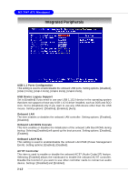
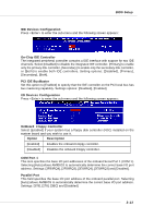
MS-7047 ATX Mainboard Advanced Chipset Features MSI Reminds You... Change these settings only if you are familiar with the chipset. Configure DRAM Timing by SPD Selects whether DRAM timing is controlled by the SPD (Serial Presence Detect) EEPROM on the DRAM module. Setting to [Auto By SPD] enables DRAM timings and the following related items to be determined by BIOS based on the configurations on the SPD. Selecting [Manual] allows users to configure the DRAM timings and the following related items manually. Setting options: [Manual], [Auto By SPD], [Turbo]. [Ultra]. SDRAM CAS# Latency This controls the timing delay (in clock cycles) before SDRAM starts a read command after receiving it. Settings: [1.5], [2.0], [2.5], [3.0]. [1.5] increases the system performance the most while [3.0] provides the most stable performance. SDRAM Bank Interleave This field selects 2-bank or 4-bank interleave for the installed SDRAM. Disable the function if 16MB SDRAM is installed. Settings: [Disabled], [2-Way] and [4-Way]. Precharge to Active (Trp) This setting controls the number of cycles for Row Address Strobe (RAS) to be allowed to precharge. If insufficient time is allowed for the RAS to accumulate its charge before DRAM refresh, refresh may be incomplete and DRAM may fail to retain data. This item applies only when synchronous DRAM is installed in the system. Setting options: [2T], [3T], [4T], [5T]. Active to Precharge (Tras) This item controls the number of cycles for Row Address Strobe (RAS) to be allowed 3-10
-
 1
1 -
2
-
3
-
4
-
5
-
6
-
7
-
8
-
9
-
10
-
11
-
12
-
13
-
14
-
15
-
16
-
17
-
18
-
19
-
20
-
21
-
22
-
23
-
24
-
25
-
26
-
27
-
28
-
29
-
30
-
31
-
32
-
33
-
34
-
35
-
36
-
37
-
38
-
39
-
 40
40 -
 41
41 -
 42
42 -
 43
43 -
 44
44 -
 45
45 -
 46
46 -
 47
47 -
 48
48 -
 49
49 -
 50
50 -
51
-
52
-
53
-
54
-
55
-
56
-
57
-
58
-
59
-
60
-
61
-
62
-
63
-
64
-
65
-
66
-
67
-
68
-
69
-
70
-
71
-
72
-
73
-
74
-
75
-
76
-
77
-
78
-
79
-
80
-
81
-
82
-
83
-
84
-
85
-
86
-
87
-
88
-
89
-
90
-
91
-
92
-
93
-
94
-
95
-
96
-
97
-
98
-
99
-
100
-
101
-
102
-
103
-
104
-
105
 |
 |
