Panasonic SL-BD20D Service Manual - Page 7
Sl-bd20, Schematic, Diagram
 |
View all Panasonic SL-BD20D manuals
Add to My Manuals
Save this manual to your list of manuals |
Page 7 highlights
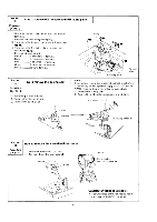
• SCHEMATIC DIAGRAM SL-BD20 FC2 To Power source 2 4,4 „j,1 A D A 03 zD ''oc zD 01- 04 SVDISR 35200V FCIOI O 2 2 8 ,j2 3 3 M 4 4 00 rest 2 4 3 26 33 45 MOTOR ASSY SM I LB02O-SM SIOI I SPEED) PIE) 2 3 4 33 rpm 11.0V OV 9.4V 7 5V 45 rpm 10.8V DV 8.2V 6.3V r I I ( R) I IL) -, ( 1 RED ( ) GRN (1 1 a WHT BLU I CARTRIDGE f-- - 7 R ch I L ch I , O CND __J • Power source circuit For [XA] area For other areas PI A 2503 T50m4 02 ,6, AC 110-127/220-240V (50/60 Hz) ATI FC I 2 u0 4 I To FC2 (AC 10V) FC3 Li A I POWER) ATI FCI 43. Oo 4 For U.S.A. and Canada: AC 120V, 60 Hz For United Kingdom and Australia: AC 240V, 50 Hz For Continental Europe: AC 220V, 50 Hz o FC2 (AC 10V) 2 FC3 A IPOWER, Notes: 1. S1: Power switch in "on" position. 2. S2: Voltage selector switch. (For [XA] area only.) 3. S101: Speed selector switch in "33" position. 4. The values are of the reference voltage for the turntable rotation of this unit, measured by a DC voltmeter (high impedance) on the basis of chassis. So, some error might be included depending on the internal impedance of the measuring instrument and the unit measured. 5. Important safety notice: Components identified by p mark have special characteristics important for safety. When replacing any of these components, use only manufacturer's specified parts. 6. VR101 is the 33-1/3 rpm speed adjustment variable resistor. 7. VR102 is the 45 rpm speed adjustment variable resistor. 8. This schematic diagram may be modified at any time with the development of new technology. • Terminal guide of diode SVD1SR35200V K A K A • Block diagram AC IN -3 T 1 II POWER O Si D1 - D4 Rectifier M DC Servo Control 1 VR 1 0 2 45 r pm 33 45 (5101) SPEED VR 1 0 1 33 rpm -7-


