Pioneer PRO-507PU Service Manual - Page 12
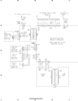
Hnm Block Diagram - power supply
 |
View all Pioneer PRO-507PU manuals
Add to My Manuals
Save this manual to your list of manuals |
Page 12 highlights
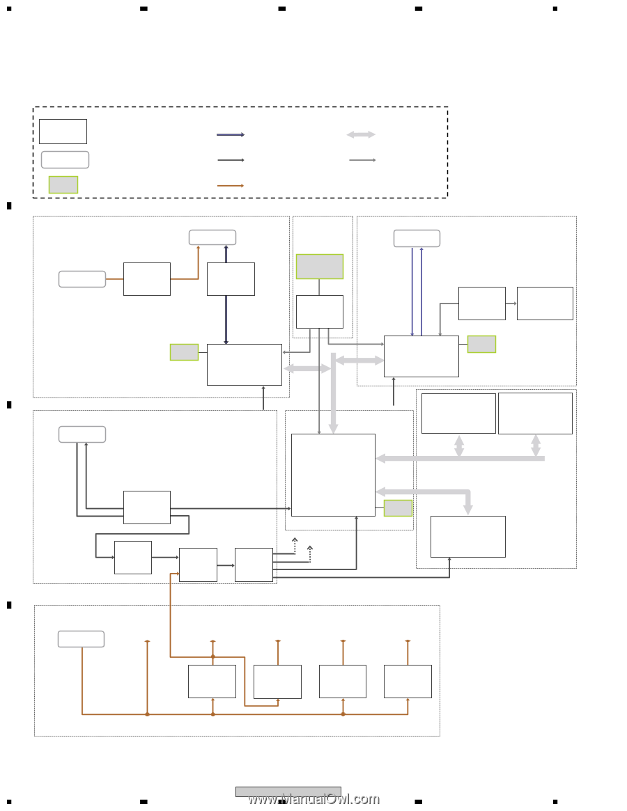
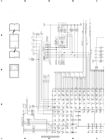
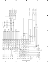
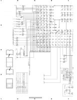
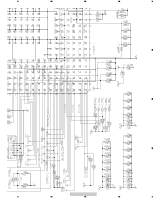
1 2 3 4 2.2 HNM BLOCK DIAGRAM • HNM Ass'y Block Diagram Classification of each component A IC xxxx IC, memory, regulator and so on CN (JA) xxxx Connector to outside of the ass'y xx MHz X'tal X'tal or oscillator Differential signal Host controll signal Power supply Bus signal Other digital signal USB block to USB Receptacle Connector CN7801 PCI clock block RJ-45 Ethernet Connector JA7752 AKP1307- Ethernet block +5V for USB Bus-power *CN7802 * Or, a wire is soldered IC7803 R5520H001B [USB High-side Switch] +5V L7801 ATH7015[C. mode filter] B directly to IC7803. X7851 ASS1211[33MHz OSC] PCI clock IC7855 CY2305SC-1H [Clock Buffer] USB Differencial signal 24MHz X'tal IC7801 VT6212L-G [USB Controller] Rx Tx IC7751 TC74LCX125 [3-state Buffer] IC7753 BR93L46RFJ-W [EEPROM (1kbit)] IC7754 RTL8100CL-LF [Ethernet Controller] Reset 25MHz X'tal Connector to Main Ass'y Reset PCI bus 8620 block IC7701 EDD2516AKTA-6B [DDR-SDRAM (256Mbit)] IC7702 EDD2516AKTA-6B [DDR-SDRAM (256Mbit)] CN7851 Memory bus IC7601 EM8620L-LFC [Digital Media Processor] Peripheral bus IC7857 C TC74LCX125 Reset [3-state Buffer] Tx / Rx I/O block IC7852 TC7S00F [NAND] IC7851 PST596IN [Reset IC] IC7852 TC74LCX04 [Inverter] Reset 27MHz X'tal IC7703 AGC1027-A-PI (S29GL128N90TFIR2) [Flash Memory (128Mbit)] Reset DDR block +5V for Power supply CN7901 +5.0V D Power supply block +3.3V +2.5V +1.2V -5.0V IC7903 LTC3412EFE [SW Reg. IC] IC7902 NJM2846DL3-25 [Regulator IC] IC7904 LTC3412EFE [SW Reg. IC] IC7901 LM2664M6X [Converter IC] 12 PRO-507PU 1 2 3 4
-
 1
1 -
2
-
3
-
4
-
5
-
6
-
 7
7 -
 8
8 -
 9
9 -
 10
10 -
 11
11 -
 12
12 -
 13
13 -
 14
14 -
 15
15 -
 16
16 -
 17
17 -
18
-
19
-
20
-
21
-
22
-
23
-
24
-
25
-
26
-
27
-
28
-
29
-
30
-
31
-
32
-
33
-
34
-
35
-
36
-
37
-
38
-
39
 |
 |