Pioneer PRO-507PU Service Manual - Page 28
Pcb Connection Diagram - main board
 |
View all Pioneer PRO-507PU manuals
Add to My Manuals
Save this manual to your list of manuals |
Page 28 highlights
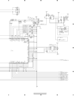
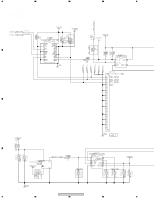
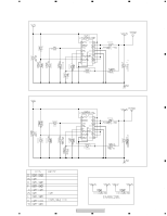
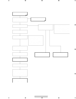
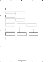
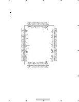
1 2 3 3. PCB CONNECTION DIAGRAM 3.1 HN MODULE ASSY A NOTE FOR PCB DIAGRAMS : 1. Part numbers in PCB diagrams match those in the schematic diagrams. 2. A comparison between the main parts of PCB and schematic diagrams is shown below. Symbol In PCB Diagrams Symbol In Schematic Diagrams B C EB C E Part Name 3. The parts mounted on this PCB include all necessary parts for several destinations. For further information for respective destinations, be sure to check with the schematic diagram. 4. View point of PCB diagrams. Connector Capacitor BCE Transistor B C EB C E SIDE A BCE Transistor with resistor DGS D G SD G S Field effect transistor P.C.Board Chip Part SIDE B Resistor array 3-terminal regulator • HN MODULE ASSY B 4 SIDE A C D 28 1 PRO-507PU 2 3 (ANP2148B) 4
-
 1
1 -
2
-
3
-
4
-
5
-
6
-
7
-
8
-
9
-
10
-
11
-
12
-
13
-
14
-
15
-
16
-
17
-
18
-
19
-
20
-
21
-
22
-
 23
23 -
 24
24 -
 25
25 -
 26
26 -
 27
27 -
 28
28 -
 29
29 -
 30
30 -
 31
31 -
 32
32 -
 33
33 -
34
-
35
-
36
-
37
-
38
-
39
 |
 |
