Seagate ST300MM0026 Savvio 10K.1 SAS Product Manual - Page 73
Compliant jitter test pattern CJTPAT
 |
View all Seagate ST300MM0026 manuals
Add to My Manuals
Save this manual to your list of manuals |
Page 73 highlights
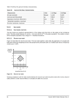
9.5.2.3.2 Receiver jitter tolerance Table 30 defines the amount of jitter the receiver shall tolerate . Table 30: Receiver jitter tolerance 1.5 Gbpsa 3.0 Gbpsa Sinusoidal jitterb,c Deterministic jittere,f,h Total jitterh Sinusoidal jitterb,d Deterministic jittere,g,h Total jitterh 0.10 0.35 0.65 0.10 0.35 0.65 a Units are in UI. b The jitter values given are normative for a combination of deterministic jitter, random jitter, and sinusoidal jitter that receivers shall be able to tolerate without exceeding a BER of 10-12. Receivers shall tolerate sinusoidal jitter of progressively greater amplitude at lower frequencies, according to the mask in figure 21 with the same deterministic jitter and random jitter levels as were used in the high frequency sweep. c Sinusoidal swept frequency: 900 kHz to > 5 MHz. d Sinusoidal swept frequency: 1.800 kHz to > 5 MHz. e No value is given for random jitter. For compliance with this standard, the actual random jitter amplitude shall be the value that brings total jitter to the stated value at a probability of 10-12. The additional 0.1 UI of sinusoidal jitter is added to ensure the receiver has sufficient operating margin in the presence of external interference. f Deterministic jitter: 900 kHz to 750 MHz. g Deterministic jitter: 1.800 kHz to 1.500 MHz. h The deterministic and total values in this table apply to jitter after application of a single pole high-pass frequency- weighting function that progressively attenuates jitter at 20 dB/decade below a frequency of ((bit rate) / 1.667). 9.5.2.3.3 Compliant jitter test pattern (CJTPAT) The CJTPAT within a compliant protocol frame is used for all jitter testing unless otherwise specified. See the SAS Interface Manual for definition of the required pattern on the physical link and information regarding special considerations for scrambling and running disparity. 9.5.2.3.4 Impedance specifications Table 31 defines impedance requirements. Table 31: Impedance requirements (Sheet 1 of 2) Requirement Time domain reflectometer rise time 20 % to 80 %a,b Media (PCB or cable) Differential impedanceb,c,d Differential impedance imbalanceb,c,d,g Common mode impedanceb,c,d Mated connectors Differential impedanceb,c,d Differential impedance imbalanceb,c,d,g Common mode impedanceb,c,d Receiver termination Differential impedanceb,e,f Differential impedance imbalanceb,e,f,g Receiver termination time constantb,e,f Units ps 1.5 Gbps 100 ohm 100 ± 10 ohm 5 ohm 32.5 ± 7.5 ohm 100 ± 15 ohm 5 ohm 32.5 ± 7.5 ohm 100 ± 15 ohm 5 ps 150 max 3.0 Gbps 50 100 ± 10 5 32.5 ± 7.5 100 ± 15 5 32.5 ± 7.5 100 ± 15 5 100 max Savvio SAS Product Manual, Rev. D 67
-
 1
1 -
2
-
3
-
4
-
5
-
6
-
7
-
8
-
9
-
10
-
11
-
12
-
13
-
14
-
15
-
16
-
17
-
18
-
19
-
20
-
21
-
22
-
23
-
24
-
25
-
26
-
27
-
28
-
29
-
30
-
31
-
32
-
33
-
34
-
35
-
36
-
37
-
38
-
39
-
40
-
41
-
42
-
43
-
44
-
45
-
46
-
47
-
48
-
49
-
50
-
51
-
52
-
53
-
54
-
55
-
56
-
57
-
58
-
59
-
60
-
61
-
62
-
63
-
64
-
65
-
66
-
67
-
 68
68 -
 69
69 -
 70
70 -
 71
71 -
 72
72 -
 73
73 -
 74
74 -
 75
75 -
 76
76 -
 77
77 -
 78
78 -
79
-
80
-
81
-
82
-
83
-
84
-
85
-
86
 |
 |
