Sharp CD-SW330 Service Manual - Page 102
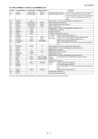
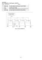
IC851 VHIAN80T53/-1: Multi Regulator AN80T53
 |
View all Sharp CD-SW330 manuals
Add to My Manuals
Save this manual to your list of manuals |
Page 102 highlights
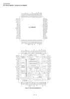
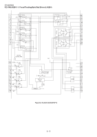
CD-SW330 IC851 VHIAN80T53/-1: Multi Regulator (AN80T53) Pin Terminal Name Function No. 1 REG4 Output 5.1 V power supply with a minimum peak out current of 1200 mA. 2 REG3 Output 13 V power supply with a minimum peak out current of 1350 mA. 3 VCC Connected to Power supplies. 4 GND Connected to the IC substrate. 5 MODE 1 REG1, REG2,REG3 and REG4 outputs are turned ON when this pin is 5 V. 6 REG2 Output 10 V power supply with a minimum peak out current of 800 mA. 7 REG1 Output 8.5 V power supply with a minimum peak out current of 700 mA. Peak Current Protection, Thermal Protection, Load Short Protection. Outputs + - Prc Drive + - Prc Drive + - Prc Drive + - Prc Drive 5 MODE1 Reference Voltage 23 REG3 VCC 13V 4 GND 1 REG4 5.1V 7 REG1 8.5V Figure 8-4: BLOCK DIAGRAM OF IC 6 REG2 10.0V 8 - 7
-
 1
1 -
2
-
3
-
4
-
5
-
6
-
7
-
8
-
9
-
10
-
11
-
12
-
13
-
14
-
15
-
16
-
17
-
18
-
19
-
20
-
21
-
22
-
23
-
24
-
25
-
26
-
27
-
28
-
29
-
30
-
31
-
32
-
33
-
34
-
35
-
36
-
37
-
38
-
39
-
40
-
41
-
42
-
43
-
44
-
45
-
46
-
47
-
48
-
49
-
50
-
51
-
52
-
53
-
54
-
55
-
56
-
57
-
58
-
59
-
60
-
61
-
62
-
63
-
64
-
65
-
66
-
67
-
68
-
69
-
70
-
71
-
72
-
73
-
74
-
75
-
76
-
77
-
78
-
79
-
80
-
81
-
82
-
83
-
84
-
85
-
86
-
87
-
88
-
89
-
90
-
91
-
92
-
93
-
94
-
95
-
96
-
 97
97 -
 98
98 -
 99
99 -
 100
100 -
 101
101 -
 102
102 -
 103
103 -
 104
104 -
 105
105 -
 106
106 -
 107
107 -
108
-
109
-
110
-
111
-
112
-
113
-
114
-
115
-
116
-
117
-
118
-
119
-
120
-
121
-
122
-
123
-
124
-
125
-
126
-
127
-
128
-
129
-
130
-
131
-
132
 |
 |
