Sharp CD-SW330 Service Manual - Page 99
Set power system GND to the minimum potential together with SGND
 |
View all Sharp CD-SW330 manuals
Add to My Manuals
Save this manual to your list of manuals |
Page 99 highlights
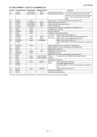
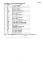
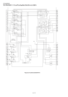
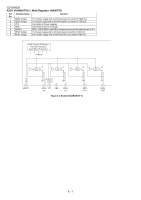
CD-SW330 IC2 VHILA6261//-1: Focus/Tracking/Spin/Sled Driver (LA6261) Pin No. Terminal Name Function 1 VO3+ BTL Output pin (+) for channel 3. 2 VO3- BTL Output pin (-) for channel 3. 3 VO2+ BTL Output pin (+) for channel 2. 4 VO2- BTL Output pin (-) for channel 2. 5 VO1+ BTL Output pin (+) for channel 1. 6 VO1- BTL Output pin (-) for channel 1. 7 PGND1 Power GND for channels 1,2,3 and 4 (BTL). 8 REGIN Regulator pin (External PNP base). 9 PVCC1 Power for channels 1,2,3 and 4 (BTL). (SVCC short-crircuited) 10 REGOUT Regulator pin (External PNP collector). 11 VIN1 Input pin for channel 1 12* VIN1G Input pin for channel 1 (for gain control) 13 VIN2 Input pin for channel 2 14* VIN2G Input pin for channel 2 (for gain control) 15 VIN3 Input pin for channel 3 16* VIN3G Input pin for channel 3 (for gain control) 17 VIN4 Input pin for channel 4 18 VIN4G Input pin for channel 4 (for gain control) 19 FWD5 CH5 Output change pin (FWD). Logic input for bridge. 20 REV5 CH5 Output change pin (REV). Logic input for bridge. 21 VCONT5 Input pin for CH5 output voltage control 22 FWD6 CH6 Output change pin (FWD). Logic input for bridge. 23 REV6 CH6 Output change pin (REV). Logic input for bridge. 24 VCONT6 Input pin for CH5 output voltage control. 25 VREFIN Reference voltage input pin. 26 SGND Signal system GND 27 SVCC Signal system power (PVCC1 short - circuited) 28 PVCC2 Power for channel 5 and 6 (H bridge). 29 MUTE Input pin for BTL mute. 30 PGND2 Power GND for channels 5 and 6 (H bridge). 31 VO6+ H bridge Output pin (+) for channel 6. 32 VO6- H bridge Output pin (-) for channel 6. 33 VO5+ H bridge Output pin (+) for channel 5. 34 VO5- H bridge Output pin (-) for channel 5. 35 VO4+ BTL Output pin (+) for channel 4. 36 VO4- BTL Output pin (-) for channel 4. In this unit, the terminal with asterisk mark (*) is (open) terminal which is not connected to the outside. * Set power system GND to the minimum potential together with SGND * Short-circuit three pins of power system SVSS and PVCC1 externally before use. 8 - 4
-
 1
1 -
2
-
3
-
4
-
5
-
6
-
7
-
8
-
9
-
10
-
11
-
12
-
13
-
14
-
15
-
16
-
17
-
18
-
19
-
20
-
21
-
22
-
23
-
24
-
25
-
26
-
27
-
28
-
29
-
30
-
31
-
32
-
33
-
34
-
35
-
36
-
37
-
38
-
39
-
40
-
41
-
42
-
43
-
44
-
45
-
46
-
47
-
48
-
49
-
50
-
51
-
52
-
53
-
54
-
55
-
56
-
57
-
58
-
59
-
60
-
61
-
62
-
63
-
64
-
65
-
66
-
67
-
68
-
69
-
70
-
71
-
72
-
73
-
74
-
75
-
76
-
77
-
78
-
79
-
80
-
81
-
82
-
83
-
84
-
85
-
86
-
87
-
88
-
89
-
90
-
91
-
92
-
93
-
 94
94 -
 95
95 -
 96
96 -
 97
97 -
 98
98 -
 99
99 -
 100
100 -
 101
101 -
 102
102 -
 103
103 -
 104
104 -
105
-
106
-
107
-
108
-
109
-
110
-
111
-
112
-
113
-
114
-
115
-
116
-
117
-
118
-
119
-
120
-
121
-
122
-
123
-
124
-
125
-
126
-
127
-
128
-
129
-
130
-
131
-
132
 |
 |