Sharp LC-15AV7U Service Manual - Page 36
Schematic Diagrams / Cba's And Test Points, Standard Notes - manual for
 |
View all Sharp LC-15AV7U manuals
Add to My Manuals
Save this manual to your list of manuals |
Page 36 highlights
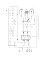
SCHEMATIC DIAGRAMS / CBA'S AND TEST POINTS NOTE: CBA AND PWB MEANS PRINTED WIRING BOARD. Standard Notes Many electrical and mechanical parts in this chassis have special characteristics. These characteristics often pass unnoticed and the protection afforded by them cannot necessarily be obtained by using replacement components rated for higher voltage, wattage, etc. Replacement parts that have these special safety characteristics are identified in this manual and its supplements; electrical components having such features are identified by the mark " # " in the schematic diagram and the parts list. Before replacing any of these components, read the parts list in this manual carefully. The use of substitute replacement parts that do not have the same safety characteristics as specified in the parts list may create shock, fire, or other hazards. Note: 1. Do not use the part number shown on these drawings for ordering. The correct part number is shown in the parts list, and may be slightly different or amended since these drawings were prepared. 2. All resistance values are indicated in ohms (K=103, M=106). 3. Resistor wattages are 1/4W or 1/6W unless otherwise specified. 4. All capacitance values are indicated in µF (P=10-6µF). 5. All voltages are DC voltages unless otherwise specified. Note of Capacitors: ML --- Mylar Cap. PP --- Metallized Film Cap. SC --- Semiconductor Cap. L --- Low Leakage type Temperature Characteristics of Capacitors are noted with the following: B --- ±10% CH --- 0±60ppm/°C CSL --- +350~-1000ppm/°C Tolerance of Capacitors are noted with the following: Z --- +80~-20% Note of Resistors: CEM --- Cement Res. MTL --- Metal Res. F --- Fuse Res. Capacitors and transistors are represented by the following symbols. CBA Symbols Schematic Diagram Symbols (Top View) (Bottom View) + Electrolytic Capacitor Digital Transistor (Bottom View) E C B (Top View) Transistor or Digital Transistor (Top View) NPN Transistor PNP Transistor E C B (Top View) NPN Digital Transistor E C B (Top View) PNP Digital Transistor E C B E C B 9-1 LCVSC
-
 1
1 -
2
-
3
-
4
-
5
-
6
-
7
-
8
-
9
-
10
-
11
-
12
-
13
-
14
-
15
-
16
-
17
-
18
-
19
-
20
-
21
-
22
-
23
-
24
-
25
-
26
-
27
-
28
-
29
-
30
-
 31
31 -
 32
32 -
 33
33 -
 34
34 -
 35
35 -
 36
36 -
 37
37 -
 38
38 -
 39
39 -
 40
40 -
 41
41 -
42
-
43
-
44
-
45
-
46
-
47
-
48
-
49
-
50
-
51
-
52
-
53
-
54
-
55
-
56
-
57
-
58
-
59
-
60
-
61
-
62
-
63
-
64
-
65
-
66
-
67
-
68
-
69
-
70
-
71
-
72
-
73
 |
 |
