Sharp XL-UH250 Service Manual - Page 89
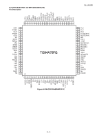
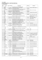
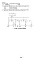
IC1 VHITC94A70FG5: CD MP3 DECODER 3/4, Pin Description
 |
View all Sharp XL-UH250 manuals
Add to My Manuals
Save this manual to your list of manuals |
Page 89 highlights
IC1 VHITC94A70FG5: CD MP3 DECODER (3/4) Pin Description Pin No. Symbol Input / Output Description 49 Pio1 Input / Output 3I/F DSP general input/output port -1. 50 Pio2 Input / Output 3I/F DSP general input/output port -2. 51 Pio3 Input / Output 3I/F DSP general input/output port -3. 52 VSS - Grounding pin for 3.3V digital circuit. 53 VDDT3 - Power supply pin for 3.3 V digital I/O circuit. 54 SBSK Output 3AI/F Sub code block sync output pin. 55 SBOK Output 3I/F CRCC check result output pin for sub code Q data. 56 IPF Output 3I/F Correction flag output. 57 SFSY Output 3I/F Servo internal register read clock output pin. 58 ZDET Output 3I/F Internal Audio DAC Zero data detection flag output. 59 GPIN Input 3I/F CD General Input port (Pull down by 100KΩ when not in use). 60 MS Input 3I/F Microprocessor I/F mode selection pin. "H": Parallel I/F, "L": Serial I/F 61 DoUT(Po6) Output 3I/F Digital Audio output (SPDIF) pin (DSP general output port -6) 62 AoUT1(Po7) Output 3I/F Audio data output pin -1 (DSP general output port -7) 63 BCKo(Po8) Output 3I/F Bit clock output pin for AoUT (DSP general output port -8) 64 LRCKo(Po9) Output 3I/F L/R channel clock output pin (DSP general output port -9) 65 AiN(Pi4) Input 3I/F Audio data input for Audio DAC (DSP general input port -4) 66 BCKi(Pi5) Input 3I/F Bit clock input pin for AiN (DSP general input port -5) 67 LRCK(Pi6) Input 3I/F L/R channel clock for AiN (DSP general input port -6) 68 VDD1 - Power supply pin for 1.5V digital circuit. 69 VSS - Grounding pin for 1.5V digital circuit. 70 AWRC Output 3AI/F VCO control pin for active wide-range PLL. 71 PVDD3 - Power supply pin for 3.3V CD PLL circuit. 72 PDo Output 3AI/F EFM and PLCK Phase difference signal output pin. 73 TMAXS Output 3AI/F TMAX detection result output pin. 74 TMAX Output 3AI/F TMAX detection result output pin. 75 LPFN Input 3AI/F PLL circuit LPF amplifier inversion input pin. 76 LPFo Output 3AI/F PLL circuit LPF amplifier Output pin. 77 PVREF 78 VCoF 79 PVSS3 80 SLCo 81 RFi 82 RFRPi 83 RFEQo - PLL circuit 1.65 V reference voltage pin. Output 3AI/F - Output 3AI/F Input 3AI/F Input 3AI/F VCO filter pin Grounding pin for 3.3V CD PLL circuit. EFM slice level output pin. Output impedance =2.5kΩ both of analog/digital slice mode. RF signal input pin Zin is selectable by command. RF ripple signal input pin. Output 3AI/F RF equalizer circuit output pin. 84 Vro 85 RESiN 86 VMDiR 87 TESTR Output 3AI/F 1.65 V reference voltage output pin. Output 3AI/F Output 3AI/F Pin for connecting a resistor for reference current generation. Reference voltage output pin for LD APC. LPF connection pin for RFEQO offset correction circuit. 8 - 5 XL-UH250 Default Remarks Input Schmitt input CMOS PORT Input Schmitt input CMOS PORT Input Output Output Output Output Output Input Schmitt input CMOS PORT For CD and DSP I/O CMOS PORT CMOS PORT CMOS PORT CMOS PORT CMOS PORT Schmitt input Input Output CMOS PORT Output CMOS PORT Output CMOS PORT Output CMOS PORT Input Schmitt input Input Schmitt input Input - Output - Output Output Output Input Output Output - Output Schmitt input Applicable in CLV/CAV mode. Connect 0.033 uF. 4-state output ( PVDD3, Hiz,PVSS3,PVREF) 3-state output (PVDD3,PVSS3,HiZ) 3-state output(PVDD3,PVSS3,HiZ) Connect resister of LPF, refer to application circuit diagram. Connect capacitor of LPF, refer to application circuit diagram. Connected to VREF and VRO inside of IC. Connect 0.1uF. Connect 0.01uF. Connect capacitor according with servo frequency band. Input Input Output Output Output Output Zin: 20kΩ, 10kΩ, 5kΩ Connect to RFRPI by 0.1uF, to RFI by 4700pF. Connected to VREF and PVREF inside of IC. Connect 0.1uF+100uF. Connect 22k//0.01uF. Connect 0.1uF. Connect more than 0.015uF.
-
 1
1 -
2
-
3
-
4
-
5
-
6
-
7
-
8
-
9
-
10
-
11
-
12
-
13
-
14
-
15
-
16
-
17
-
18
-
19
-
20
-
21
-
22
-
23
-
24
-
25
-
26
-
27
-
28
-
29
-
30
-
31
-
32
-
33
-
34
-
35
-
36
-
37
-
38
-
39
-
40
-
41
-
42
-
43
-
44
-
45
-
46
-
47
-
48
-
49
-
50
-
51
-
52
-
53
-
54
-
55
-
56
-
57
-
58
-
59
-
60
-
61
-
62
-
63
-
64
-
65
-
66
-
67
-
68
-
69
-
70
-
71
-
72
-
73
-
74
-
75
-
76
-
77
-
78
-
79
-
80
-
81
-
82
-
83
-
 84
84 -
 85
85 -
 86
86 -
 87
87 -
 88
88 -
 89
89 -
 90
90 -
 91
91 -
 92
92 -
 93
93 -
 94
94 -
95
-
96
-
97
-
98
-
99
-
100
-
101
-
102
-
103
-
104
-
105
-
106
-
107
-
108
-
109
-
110
-
111
-
112
-
113
-
114
-
115
-
116
 |
 |
