Sharp XL-UH250 Service Manual - Page 90
IC1 VHITC94A70FG5: CD MP3 DECODER 4/4, Pin Description
 |
View all Sharp XL-UH250 manuals
Add to My Manuals
Save this manual to your list of manuals |
Page 90 highlights
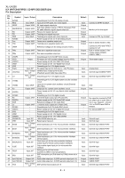
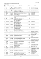
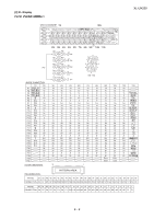
XL-UH250 IC1 VHITC94A70FG5: CD MP3 DECODER (4/4) Pin Description Pin No. Symbol 88 AGCi Input / Output Description Input 3AI/F RF signal AGC amplifier input pin. Default Input Remarks 89 Rfo Output 3AI/F RF signal generation amplifier output pin. Output 90 RVDD3 Power supply for 3.3V RF amplifier core circuit. 91 LDo 92 MDi 93 RVSS3 94 FNi2 95 FNi1 96 FPi2 97 FPi1 98 TPi 99 TNPC 100 TNi Output 3AI/F Input 3AI/F Input 3AI/F Input 3AI/F Input 3AI/F Input 3AI/F Input 3AI/F Output 3AI/F Input 3AI/F Laser diode amplifier output pin. Monitor photodiode amplifier input pin. Grounding pin for RF amplifier core circuit. Main beam signal input pin. To be connected to PIN diode C. Main beam signal input pin. To be connected to PIN diode A. Main beam signal input pin. To be connected to PIN diode D. Main beam signal input pin. To be connected to PIN diode B. Sub beam signal input pin. To be connected to PIN diode F. TNI/TPI input common capacitor connection pin. Sub beam signal input pin. To be connected to PIN diode E. Input Reference Voltage=178mVtyp. Input Input Input Input Input Output Input Connect to VRO by capacitor. * 3A I/F : 3 V analog circuit input/output pin. 1.5 I/F : 1.5Vdigital input/output pin. 3 I/F : 3 V digital input/output pin. Note: The servo output pins (FOO, TRO, FMO, and DMO) become undefined or GND level under the following conditions: • /RST pin = Low • Crystal oscillation stopped according to the instructions by the Stop crystal oscillation command. • Power supply for CD is OFF. • SRAMSTB pin = High To prevent the undefined pin states from affecting the servo circuitry or any other mechanical blocks in the system, appropriate measures should be taken, such as using a driver IC supporting a standby feature to place the system in standby mode while either of the above conditions is satisfied. 8 - 6
-
 1
1 -
2
-
3
-
4
-
5
-
6
-
7
-
8
-
9
-
10
-
11
-
12
-
13
-
14
-
15
-
16
-
17
-
18
-
19
-
20
-
21
-
22
-
23
-
24
-
25
-
26
-
27
-
28
-
29
-
30
-
31
-
32
-
33
-
34
-
35
-
36
-
37
-
38
-
39
-
40
-
41
-
42
-
43
-
44
-
45
-
46
-
47
-
48
-
49
-
50
-
51
-
52
-
53
-
54
-
55
-
56
-
57
-
58
-
59
-
60
-
61
-
62
-
63
-
64
-
65
-
66
-
67
-
68
-
69
-
70
-
71
-
72
-
73
-
74
-
75
-
76
-
77
-
78
-
79
-
80
-
81
-
82
-
83
-
84
-
 85
85 -
 86
86 -
 87
87 -
 88
88 -
 89
89 -
 90
90 -
 91
91 -
 92
92 -
 93
93 -
 94
94 -
 95
95 -
96
-
97
-
98
-
99
-
100
-
101
-
102
-
103
-
104
-
105
-
106
-
107
-
108
-
109
-
110
-
111
-
112
-
113
-
114
-
115
-
116
 |
 |
