Sony DSC-W80/W Sony® Guide to Digital Photography (Spring 2007) - Page 13
ony im - windows 7
 |
View all Sony DSC-W80/W manuals
Add to My Manuals
Save this manual to your list of manuals |
Page 13 highlights
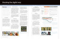
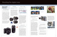
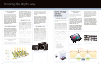
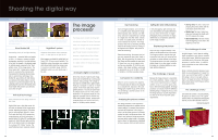
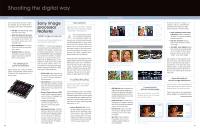
Shooting the digital way CAMERA SYSTEMS Charge Coupled Device (CCD) sensors CCD stands for Charge Coupled Device. It's often compared to a bucket brigade. When light enters the "bucket" of a pixel's image sensing area, the light generates an electrical charge. After the exposure, charges are passed along to other buckets, and then to an amplifier that converts the charges to a voltage. CCDs exhibit high image quality, with a minimum of unwanted image mottling or "noise." The challenge of resolution Together with the lens, the image sensor is primarily responsible for achieving high resolution. The number of pixels in the image sensor generally determines the maximum number of pixels in the recorded image. This encourages CCD manufacturers to squeeze smaller and smaller pixels into a given image sensor size. But smaller pixels come at a cost: sensitivity and noise. The challenge of sensitivity and noise Smaller pixels represent smaller "buckets" in which to collect electric charge. Other things being equal, smaller pixels have less "sensitivity" to light: they require more light to achieve a given picture quality. In addition, other things being equal, smaller pixels are more prone to mottling in the picture, the random flecks and specks of picture "noise." The importance of size Small pixels give you resolution. Big pixels give you high sensitivity and low noise. It's a classic engineering tradeoff. One obvious way to overcome this is to increase the overall size of the image sensor. While rarely prominent on the spec sheet, image sensor size is just as important as the number of megapixels. Sensors are classified by "type," measured in fractions of an inch. Other things being equal, each pixel in a 2/3-inch image sensor will be four times the size of a pixel in a 1/3-inch type image sensor for dramatic improvements in sensitivity and noise. Larger image sensors also help you control depth of field to achieve "selective focus." This creative tool helps your subject stand out by blurring the background. The geometry of large image sensors makes them inherently better suited to selective focus than small sensors. You can choose to open the iris to blur the background. Or stop the iris down to keep the entire scene tack-sharp. The inch "types" date back to the outside diameter of the pickup tubes of old broadcast television cameras. This outside diameter was always much larger than the inside target size. This has created a paradox. Nothing about a modern 2/3-inch type integrated circuit image sensor actually measures 2/3-inch! The challenge of dust The image sensors of digital SLRs face one challenge that the sensors of lensintegral cameras never see. When you take off the lens of a D-SLR, you expose the image sensor to environmental dust. Image sensor pixels are microscopically small, from two to six micrometers across. In comparison, dust motes can be huge: 40 micrometers across. So when a single dust mote alights on the image sensor, it can obscure many, many pixels. And once dust has landed on the image sensor, it is surprisingly difficult to remove. KEY Accumulating Bucket Carrying Bucket Charge Vertical Register Horizontal Register Amplifier Signal Output LIGHT Operating principle of an "interline transfer" CCD image sensor. Buckets of charge in the light-sensing area are transferred into the vertical registers, from which they go to a horizontal register and the amplifier. 22 Take the lens off a digital SLR and you'll quickly realize why anti-dust technology is so important. CAMERA SYSTEMS Sony image sensor features Full APS-size image sensor Achieving the ultimate in picture quality in the a100. If you want professional-grade resolution, sensitivity and freedom from noise, there's simply no substitute for a professional-size image sensor. That's why the Sony a100 Digital SLR incorporates a sensor with a live image area almost the exactly the same size as the APS-C film frame: 23.6 x 15.8 mm. To appreciate the APS advantage, compare the a100 with a typical 5.1 megapixel camera using a 1/2.5-inch type sensor (live image area 5.76 x 4.29 mm). The a100 sensor has more than fifteen times the area of this typical sensor. And even though the a100 has twice as many pixels, each a100 pixel has more than seven times the area of the typical pixel! The larger image sensor has dramatic advantages: • Higher resolution • Higher sensitivity • Lower image noise • Greater exposure latitude • More selective focus Sony Super HAD™ CCD image sensor Incredible resolution, sensitivity and clarity from the industry leader in CCD image sensors - Sony. Sony is not only the industry leader in charge coupled device (CCD) image sensors, we supply more digital camera CCDs than all other companies combined! This expertise, unrivaled in the industry, is evident in our proprietary Super HAD™ CCDs. Sony uses a Hole Accumulated Diode (HAD) design to achieve not only high resolution but also low noise and superb low-light sensitivity. The CCD structure alternates between small light-sensitive windows and transfer sections that provide DC voltage and output connections. To maximize sensitivity, the Sony design uses an array of microlenses on the CCD surface to gather the light that might otherwise miss the light-sensitive areas. And Sony CCD technology continues to advance. Sony refinements to the silicon substrate enable succeeding generations of Sony digital cameras to "have their cake and eat it, too." Each generation features more megapixels, while maintaining or improving sensitivity and noise performance. An engineering marvel, the Sony 10.2 Megapixel Super HAD CCD. Previous microlens designs (left) miss some of the incoming light. Our Super HAD design (right) gathers more light for even higher sensitivity. ON-CHIP MICROLENS Light Ineffective Effective Photo shielding AI The a100 image sensor has more than fifteen times the image area of the typical 1/2.5-inch type sensor. TRANSFER SECTION SENSOR TRANSFER SECTION The Sony microlenses maximize low-light performance by directing light onto the sensor areas and away from the non-sensing transfer sections. 23
-
 1
1 -
2
-
3
-
4
-
5
-
6
-
7
-
 8
8 -
 9
9 -
 10
10 -
 11
11 -
 12
12 -
 13
13 -
 14
14 -
 15
15 -
 16
16 -
 17
17 -
 18
18 -
19
-
20
-
21
-
22
-
23
-
24
-
25
-
26
-
27
-
28
-
29
-
30
-
31
 |
 |
