Sony ICF-SW7600GR Service Manual - Page 11
Printed Wiring Board – Main Board (component Side) –
 |
UPC - 027242580084
View all Sony ICF-SW7600GR manuals
Add to My Manuals
Save this manual to your list of manuals |
Page 11 highlights
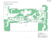
4-3. PRINTED WIRING BOARD - MAIN BOARD (COMPONENT SIDE) - A MAIN BOARD (COMPONENT SIDE) B ICF-SW7600GR C D E F US G B H TO KEY BOARD I 11 1-679-368- (11) 15 16 17 18 19 20 21 22 23 24 25 26 27 28 11 11 Note on Printed Wiring Boards: • X : parts extracted from the component side. • a : Through hole. • : Pattern from the side which enables seeing. (The other layers' patterns are not indicated.) Caution: Pattern face side: (Conductor Side) Parts face side: (Component Side) Parts on the pattern face side seen from the pattern face are indicated. Parts on the parts face side seen from the parts face are indicated.
-
 1
1 -
2
-
3
-
4
-
5
-
 6
6 -
 7
7 -
 8
8 -
 9
9 -
 10
10 -
 11
11 -
 12
12 -
 13
13 -
 14
14 -
 15
15 -
 16
16 -
17
-
18
-
19
-
20
-
21
-
22
-
23
-
24
-
25
-
26
 |
 |

11
11
ICF-SW7600GR
4-3. PRINTED WIRING BOARD – MAIN BOARD (COMPONENT SIDE) –
15
16
A
B
C
D
E
F
G
H
I
17
18
19
20
21
22
23
24
25
26
27
28
MAIN BOARD
(COMPONENT SIDE)
1-679-368-
11
(11)
B
TO
KEY BOARD
US
Note on Printed Wiring Boards:
•
X
: parts extracted from the component side.
•
a
: Through hole.
•
: Pattern from the side which enables seeing.
(The other layers' patterns are not indicated.)
Caution:
Pattern face side:
Parts on the pattern face side seen from
(Conductor Side)
the pattern face are indicated.
Parts face side:
Parts on the parts face side seen from
(Component Side)
the parts face are indicated.