Sony ICF-SW7600GR Service Manual - Page 15
Schematic Diagram – Key Board –, Waveform
 |
UPC - 027242580084
View all Sony ICF-SW7600GR manuals
Add to My Manuals
Save this manual to your list of manuals |
Page 15 highlights
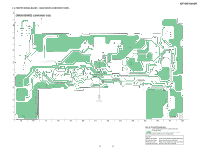
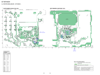
4-7. SCHEMATIC DIAGRAM - KEY BOARD - • Refer to page 16 for IC Pin Function. ICF-SW7600GR 1 • WAVEFORM 1 IC302 wf 13.3 µs 15 1.8 Vp-p 15 Note on Schematic Diagram: • All capacitors are in µF unless otherwise noted. pF: µµF 50 WV or less are not indicated except for electrolytics and tantalums. • All resistors are in Ω and 1/4 W or less unless otherwise specified. • C : panel designation. • A : B+ Line. • H : adjustment for repair. • Voltages and waveforms are dc with respect to ground under no-signal (detuned) conditions. • Voltages are taken with a VOM (Input impedance 10 MΩ). Voltage variations may be noted due to normal production tolerances. • Voltage variations may be noted due to normal production tolerances. • Abbreviation CH : Chinese model
-
 1
1 -
2
-
3
-
4
-
5
-
6
-
7
-
8
-
9
-
 10
10 -
 11
11 -
 12
12 -
 13
13 -
 14
14 -
 15
15 -
 16
16 -
 17
17 -
 18
18 -
 19
19 -
 20
20 -
21
-
22
-
23
-
24
-
25
-
26
 |
 |
