Asus P5PEVM Motherboard Installation Guide - Page 60
Chipset - no display
 |
View all Asus P5PEVM manuals
Add to My Manuals
Save this manual to your list of manuals |
Page 60 highlights
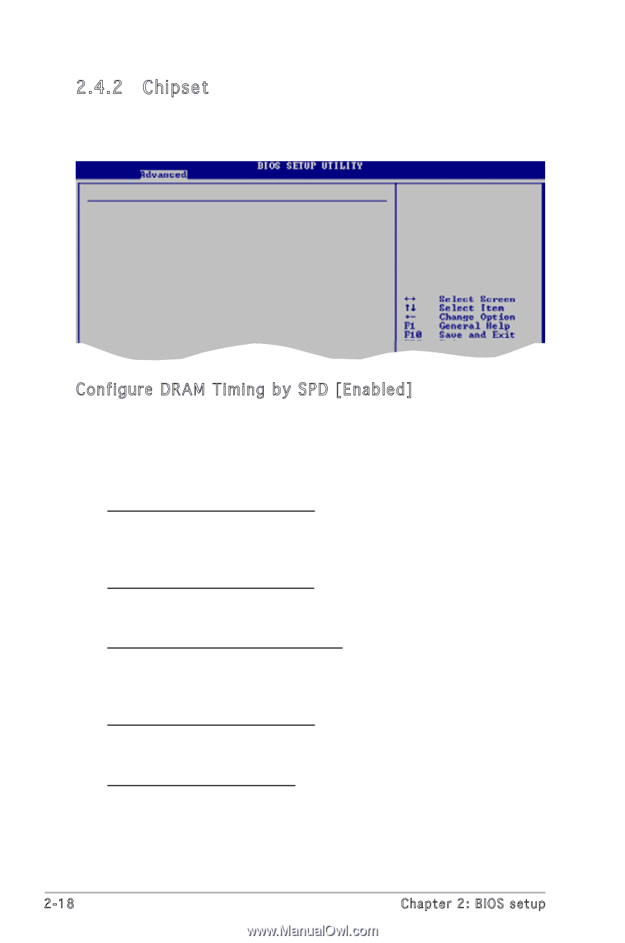
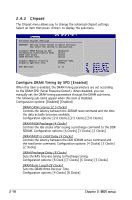
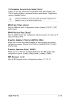
2.4.2 Chipset The Chipset menu allows you to change the advanced chipset settings. Select an item then press to display the sub-menu. Advanced Chipset Settings WARNING: Setting wrong values in below sections may cause the system to malfunction. Configure DRAM Timing by SPD [Enabled] Performance Acceleration Mode [Auto] DRAM Idle Timer [Auto] DRAM Refresh Rate [Auto] Graphic Adapter Priority [AGP/Int-VGA] Graphics Aperture Size [64MB] MPS Revision [1.4] Configure DRAM Timing by SPD [Enabled] When this item is enabled, the DRAM timing parameters are set according to the DRAM SPD (Serial Presence Detect). When disabled, you can manually set the DRAM timing parameters through the DRAM sub-items. The following sub-items appear when this item is Disabled. Configuration options: [Disabled] [Enabled] DRAM CAS# Latency [2.5 Clocks] Controls the latency between the SDRAM read command and the time the data actually becomes available. Configuration options: [2.0 Clocks] [2.5 Clocks] [3.0 Clocks] DRAM RAS# Precharge [4 Clocks] Controls the idle clocks after issuing a precharge command to the DDR SDRAM. Configuration options: [4 Clocks] [3 Clocks] [2 Clocks] DRAM RAS# to CAS# Delay [4 Clocks] Controls the latency between the DDR SDRAM active command and the read/write command. Configuration options: [4 Clocks] [3 Clocks] [2 Clocks] DRAM Precharge Delay [8 Clocks] Sets the RAS Activate timing to Precharge timing. Configuration options: [8 Clock] [7 Clocks] [6 Clocks] [5 Clocks] DRAM Burst Length [8 Clocks] Sets the DRAM Write Recover Time. Configuration options: [4 Clocks] [8 Clocks] 2-18 Chapter 2: BIOS setup
-
 1
1 -
2
-
3
-
4
-
5
-
6
-
7
-
8
-
9
-
10
-
11
-
12
-
13
-
14
-
15
-
16
-
17
-
18
-
19
-
20
-
21
-
22
-
23
-
24
-
25
-
26
-
27
-
28
-
29
-
30
-
31
-
32
-
33
-
34
-
35
-
36
-
37
-
38
-
39
-
40
-
41
-
42
-
43
-
44
-
45
-
46
-
47
-
48
-
49
-
50
-
51
-
52
-
53
-
54
-
 55
55 -
 56
56 -
 57
57 -
 58
58 -
 59
59 -
 60
60 -
 61
61 -
 62
62 -
 63
63 -
 64
64 -
 65
65 -
66
-
67
-
68
-
69
-
70
-
71
-
72
-
73
-
74
-
75
-
76
-
77
-
78
-
79
-
80
 |
 |