Gigabyte GA-H110TN-M User Manual - Page 16
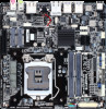
GPIO GPIO Header, LVDS LVDS Header, Only for GA-H110TN-M.
 |
View all Gigabyte GA-H110TN-M manuals
Add to My Manuals
Save this manual to your list of manuals |
Page 16 highlights
10) GPIO (GPIO Header)j This header allows for control of high and low signals. Pin No. Definition 10 9 1 IO_GP70 2 IO_GP71 3 IO_GP72 21 4 IO_GP73 5 IO_GP74 Pin No. 6 7 8 9 10 Definition IO_GP75 IO_GP76 IO_GP77 GP_IN_OUT GND 11) LVDS (LVDS Header) LVDS stands for Low-voltage differential signaling, which uses high-speed analog circuit techniques to provide multigigabit data transfers on copper interconnects and is a generic interface standard for highspeed data transmission. 2 1 40 39 Pin No. 1 2 3 4 5 6 7 8 9 10 11 12 13 14 15 16 17 18 19 20 Definition LCD_VCC LCD_VCC VCC3 NC NC -RXO0_C +RXO0_C GND -RXO1_C +RXO1_C GND -RXO2_C +RXO2_C GND -RXO3_C +RXO3_C GND -RXECLKO_C +RXECLKO_C GND Pin No. 21 22 23 24 25 26 27 28 29 30 31 32 33 34 35 36 37 38 39 40 Definition -RXE0_C +RXE0_C GND -RXE1_C +RXE1_C GND -RXE2_C +RXE2_C CABLE_DET (Note) -RXE3_C +RXE3_C GND -RXECLKE_C +RXECLKE_C GND SC_BKLT_EN SC_BKLT_CTL FPD_PWR FPD_PWR FPD_PWR (Note) Connects to Pin 35 and the ground pin of the LVDS. j Only for GA-H110TN-M. - 16 -
-
 1
1 -
2
-
3
-
4
-
5
-
6
-
7
-
8
-
9
-
10
-
 11
11 -
 12
12 -
 13
13 -
 14
14 -
 15
15 -
 16
16 -
 17
17 -
 18
18 -
 19
19 -
 20
20 -
 21
21 -
22
-
23
-
24
-
25
-
26
-
27
-
28
-
29
-
30
-
31
-
32
-
33
-
34
-
35
-
36
-
37
-
38
-
39
-
40
-
41
 |
 |
