Intel DP67BG Product Specification - Page 7
Regulatory Compliance and Battery Disposal Information, s, Tables - usb 3
 |
View all Intel DP67BG manuals
Add to My Manuals
Save this manual to your list of manuals |
Page 7 highlights
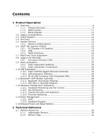
Contents 5 Regulatory Compliance and Battery Disposal Information 5.1 Regulatory Compliance 79 5.1.1 Safety Standards 79 5.1.2 European Union Declaration of Conformity Statement 80 5.1.3 Product Ecology Statements 81 5.1.4 EMC Regulations 83 265H 5.1.5 ENERGY STAR* 5.0, e-Standby, and ErP Compliance 86 86H 26H 5.1.6 Regulatory Compliance Marks (Board Level 87 87H 267H 5.2 Battery Disposal Information 88 8H 268H Figures 1. Major Board Components 11 89H 269H 2. Block Diagram 13 90H 270H 3. Memory Channel and DIMM Configuration 18 91H 271H 4. Back Panel Audio Connectors 23 92H 27H 5. LAN Connector LED Locations 25 93H 273H 6. Thermal Sensors and Fan Headers 28 94H 274H 7. Location of Diagnostic LEDs 35 95H 275H 8. Location of the Onboard Power and Reset Buttons 37 96H 276H 9. Detailed System Memory Address Map 40 97H 27H 10. Back Panel Connectors 42 98H 278H 11. Component-side Connectors and Headers 43 9H 279H 12. Connection Diagram for Front Panel Header 49 10H 280H 13. Connection Diagram for Front Panel USB Headers 51 10H 281H 14. Location of the Jumper Block 52 102H 28H 15. Board Dimensions 54 103H 283H 16. Localized High Temperature Zones 58 104H 284H Tables 1. Feature Summary 9 105H 285H 2. Components Shown in Figure 1 12 106H 286H 3. Supported Memory Configurations 16 107H 287H 4. Audio Jack Support 22 108H 28H 5. LAN Connector LED States 25 109H 289H 6. Effects of Pressing the Power Switch 29 10H 290H 7. Power States and Targeted System Power 30 1H 291H 8. Wake-up Devices and Events 31 12H 29H 9. Diagnostic LEDs 36 13H 293H 10. System Memory Map 41 14H 294H 11. Component-side Connectors and Headers Shown in Figure 11 44 15H 295H 12. IEEE 1394a Header 45 16H 296H 13. Front Panel Audio Header 45 17H 297H 14. SATA Connectors 45 18H 298H 15. S/PDIF Header 45 19H 29H 16. Chassis Intrusion Header 46 120H 30H vii
-
 1
1 -
 2
2 -
 3
3 -
 4
4 -
 5
5 -
 6
6 -
 7
7 -
 8
8 -
 9
9 -
 10
10 -
 11
11 -
 12
12 -
13
-
14
-
15
-
16
-
17
-
18
-
19
-
20
-
21
-
22
-
23
-
24
-
25
-
26
-
27
-
28
-
29
-
30
-
31
-
32
-
33
-
34
-
35
-
36
-
37
-
38
-
39
-
40
-
41
-
42
-
43
-
44
-
45
-
46
-
47
-
48
-
49
-
50
-
51
-
52
-
53
-
54
-
55
-
56
-
57
-
58
-
59
-
60
-
61
-
62
-
63
-
64
-
65
-
66
-
67
-
68
-
69
-
70
-
71
-
72
-
73
-
74
-
75
-
76
-
77
-
78
-
79
-
80
-
81
-
82
-
83
-
84
-
85
-
86
-
87
-
88
-
89
-
90
-
91
 |
 |