Nintendo 1504166 Programming Manual - Page 142
UART Communication Functions, a fixed 1 bit.
 |
View all Nintendo 1504166 manuals
Add to My Manuals
Save this manual to your list of manuals |
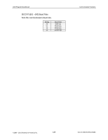
Page 142 highlights
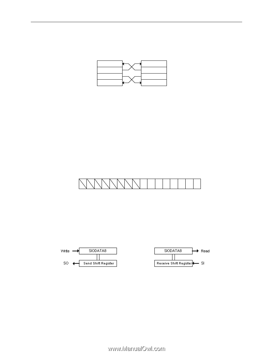
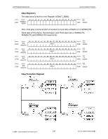
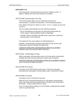
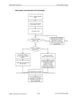
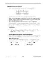
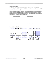
AGB Programming Manual Communication Functions 13.3 UART Communication Functions UART communications can be illustrated using the following drawing. SI SI SO SO SD SD SC SC In UART communication mode, a HI level is output from the SD terminal. When the receive data register (or the receive FIFO) is full, a HI is output from the SD terminal. When it is not full, a LO is output from the SD terminal if the receive enable flag is set. A HI is output if it is reset. The output of the SD terminal of the other machine is input to the SC terminal. Once data is written to the send data register, data is sent after a "Start bit" (1 bit) is sent from the SO terminal. However, when the CTS flag for the Control Register is set, data can be sent only when there is a LO input to the SC terminal. The Stop bit is a fixed 1 bit. Data Register Address 12Ah Register SIO DATA8 15 14 13 12 11 10 09 08 07 06 05 04 03 02 01 00 Attributes R/W Initial Value 0000h Relations Between Data Register, FIFO, and Shift Register When sending or receiving, there are 4 bytes of FIFO. By using the FIFO enable flag for the control register SIOCNT, you can select whether to use or not use FIFO. When FIFO is not Used If written to a data register SIODATA8, data is written to a send shift register, and if read, data is read from a receive shift register. (Only the lower 8 bits are valid.) ©1999 - 2001 Nintendo of America Inc. 142 D.C.N. AGB-06-0001-002B4
-
 1
1 -
2
-
3
-
4
-
5
-
6
-
7
-
8
-
9
-
10
-
11
-
12
-
13
-
14
-
15
-
16
-
17
-
18
-
19
-
20
-
21
-
22
-
23
-
24
-
25
-
26
-
27
-
28
-
29
-
30
-
31
-
32
-
33
-
34
-
35
-
36
-
37
-
38
-
39
-
40
-
41
-
42
-
43
-
44
-
45
-
46
-
47
-
48
-
49
-
50
-
51
-
52
-
53
-
54
-
55
-
56
-
57
-
58
-
59
-
60
-
61
-
62
-
63
-
64
-
65
-
66
-
67
-
68
-
69
-
70
-
71
-
72
-
73
-
74
-
75
-
76
-
77
-
78
-
79
-
80
-
81
-
82
-
83
-
84
-
85
-
86
-
87
-
88
-
89
-
90
-
91
-
92
-
93
-
94
-
95
-
96
-
97
-
98
-
99
-
100
-
101
-
102
-
103
-
104
-
105
-
106
-
107
-
108
-
109
-
110
-
111
-
112
-
113
-
114
-
115
-
116
-
117
-
118
-
119
-
120
-
121
-
122
-
123
-
124
-
125
-
126
-
127
-
128
-
129
-
130
-
131
-
132
-
133
-
134
-
135
-
136
-
 137
137 -
 138
138 -
 139
139 -
 140
140 -
 141
141 -
 142
142 -
 143
143 -
 144
144 -
 145
145 -
 146
146 -
 147
147 -
148
-
149
-
150
-
151
-
152
-
153
-
154
-
155
-
156
-
157
-
158
-
159
-
160
-
161
-
162
-
163
-
164
-
165
-
166
-
167
-
168
-
169
-
170
-
171
 |
 |