Sony HCD-HX7 Service Manual - Page 54
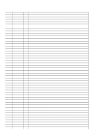
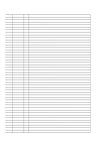
Pin No., Pin Name, Description
 |
View all Sony HCD-HX7 manuals
Add to My Manuals
Save this manual to your list of manuals |
Page 54 highlights
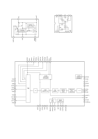
HCD-HX3/HX5/HX7 Pin No. 44 45 46 47 48 49, 50 51 52 53 54 55 56 57 58 59 60 61 62 63 64 65 66 67 68 69 70 71 72 73 74 75 76 77 78 79 80 81 82 83 84 85 86 87 88 89 90 Pin Name TEST IRQ AoUT3 (PO4) AoUT2 (PO5) PIO0 PIO1, PIO2 PIO3 VSS1 VDDT3 SBSY SBOK/FOK IPF SFSY/LOCK ZDET GPIN MS DOUT (PO6) AOUT (PO7) BCK (PO8) LRCK (PO9) AIN (PI4) BCKi (PI5) LRCKi (PI6) VDD1 VSS AWRC PVDD3 PDO TMAXS TMAX LPFN LPFo PVREF VCOF PVSS3 SLCo RFi RFRPi RFEQo VRo RESiN VMDiR TESTR AGCi RFo RVDD3 I/O Description I Setting terminal for test mode Normally fixed at "L" I Interrupt request signal input terminal Not used O Request signal output to the USB controller (HX3/HX5) O Audio data output terminal Not used O Request signal output to the system controller and USB controller (HX3/HX5) Request signal output to the system controller (HX7) O Not used I Gate signal input from the USB controller (HX3/HX5) - Ground terminal - Power supply terminal (+3.3 V) O Subcode block sync signal output to the system controller O Not used O Not used O Not used O Zero detection signal output terminal Not used I Not used I Microcomputer interface mode selection signal input terminal Fixed at "H" in this set O Digital audio data output terminal Not used O Audio data output terminal Not used O Bit clock signal output terminal Not used O L/R sampling clock signal output terminal Not used I Digital audio data input from USB controller (HX3/HX5) I Bit clock signal input from the USB controller (HX3/HX5) I L/R sampling clock signal input from the USB controller (HX3/HX5) - Power supply terminal (+1.5 V) - Ground terminal - Not used - Power supply terminal (+3.3 V) O Phase error margin signal between EFM signal and PLCK signal output terminal O TMAX detection signal output terminal Not used O TMAX detection signal output terminal I Inverted signal input from the operation amplifier for PLL loop filter O Signal output from the operation amplifier for PLL loop filter I Reference voltage (+1.65V) input terminal O VCO filter output terminal - Ground terminal O EFM slice level output terminal I RF signal input terminal I RF ripple signal input terminal O EFM slice level output terminal O Reference voltage (+1.65V) output terminal O External resistor connection terminal O Reference voltage (+1.65V) output terminal for automatic power control circuit O Low-pass filter terminal for RFEQO offset correction I RF signal amplitude adjustment amplification input terminal O RF signal generation amplification output terminal - Power supply terminal (+3.3 V) 54
-
 1
1 -
2
-
3
-
4
-
5
-
6
-
7
-
8
-
9
-
10
-
11
-
12
-
13
-
14
-
15
-
16
-
17
-
18
-
19
-
20
-
21
-
22
-
23
-
24
-
25
-
26
-
27
-
28
-
29
-
30
-
31
-
32
-
33
-
34
-
35
-
36
-
37
-
38
-
39
-
40
-
41
-
42
-
43
-
44
-
45
-
46
-
47
-
48
-
 49
49 -
 50
50 -
 51
51 -
 52
52 -
 53
53 -
 54
54 -
 55
55 -
 56
56 -
 57
57 -
 58
58 -
 59
59 -
60
-
61
-
62
-
63
-
64
-
65
-
66
-
67
-
68
-
69
-
70
-
71
-
72
-
73
-
74
-
75
-
76
-
77
-
78
-
79
-
80
-
81
-
82
-
83
-
84
-
85
-
86
-
87
-
88
-
89
-
90
 |
 |
