Via EPIA-EK10000G User Manual - Page 67
DRAM Clock, DRAM Timing
 |
UPC - 825529003581
View all Via EPIA-EK10000G manuals
Add to My Manuals
Save this manual to your list of manuals |
Page 67 highlights
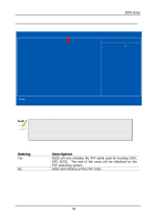
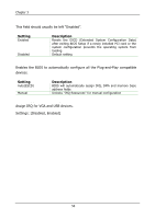
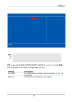
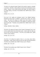
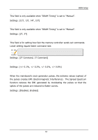
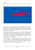
FREQUENCY / VOLTAGE CONTROL BIOS Setup Phoenix - AwardBIOS CMOS Setup Utility Frequency / Voltage Control DRAM Clock DRAM Timing SDRAM CAS Latency Bank Interleave Precharge to Active(Trp) Active to Precharge(Tras) Active to CMD(Trcd) REF to ACT/REF to REF(Trfc ACT(0) to ACT(1) (TRRD) DRAM Command Rate Spread Spectrum Range [By SPD] [Auto By SPD] 2.5 Disabled 4T 9T 4T 15T 3T [2T Command] [+/- 0.3%] Item Help Menu Level Spread Spectrum [Enabled] : Move Enter: Select +/-/PU/PD: Value F10: Save F5: Previous Values F6: Fail-Safe Defaults ESC: Exit F1: General Help F7: Optimized Defaults DRAM Clock The chipset supports synchronous and asynchronous mode between host clock and DRAM clock frequency. Settings: [100 MHz, 133 MHz, 166 MHz, 200MHz, By SPD] DRAM Timing The value in this field depends on the memory modules installed in your system. Changing the value from the factory setting is not recommended unless you install new memory that has a different performance rating than the original modules. Settings: [Manual, Auto By SPD] 59
-
 1
1 -
2
-
3
-
4
-
5
-
6
-
7
-
8
-
9
-
10
-
11
-
12
-
13
-
14
-
15
-
16
-
17
-
18
-
19
-
20
-
21
-
22
-
23
-
24
-
25
-
26
-
27
-
28
-
29
-
30
-
31
-
32
-
33
-
34
-
35
-
36
-
37
-
38
-
39
-
40
-
41
-
42
-
43
-
44
-
45
-
46
-
47
-
48
-
49
-
50
-
51
-
52
-
53
-
54
-
55
-
56
-
57
-
58
-
59
-
60
-
61
-
 62
62 -
 63
63 -
 64
64 -
 65
65 -
 66
66 -
 67
67 -
 68
68 -
 69
69 -
 70
70 -
 71
71 -
 72
72 -
73
-
74
-
75
-
76
-
77
-
78
-
79
 |
 |