ASRock K8S8X User Manual - Page 32
Memory Controller Configuration, 7.1.1, Memory Configuration
 |
View all ASRock K8S8X manuals
Add to My Manuals
Save this manual to your list of manuals |
Page 32 highlights
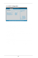
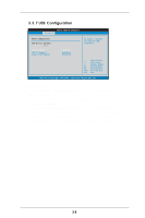
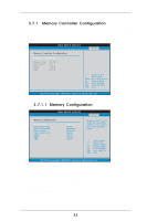
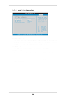
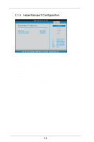
3.7.1 Memory Controller Configuration In this section, it will display the status of memory clock, CAS Latency, TRCD, TRAS, and TRP. You may also set the memory configuration in the sub-screen under this section. BIOS SETUP UTILITY Memory Controller Configuration Memory Configuration Memory CLK CAS Latency TRCD TRAS TRP : 166 MHz : 3.0 : 4 CLK : 7 CLK : 4 CLK Chipset Select Screen Select Item Enter Go to Sub Screen F1 General Help F9 Load Defaults F10 Save and Exit ESC Exit v02.54 (C) Copyright 1985-2003, American Megatrends, Inc. 3.7.1.1 Memory Configuration BIOS SETUP UTILITY Memory Configuration Memory Clock Bank Interleaving Node Interleaving Burst Length CAS Latency (CL) TRCD TRAS TRP [Auto] [Auto] [Disabled] [8 Beats] [Auto] [Auto] [Auto] [Auto] Chipset Memory Clock can be set by the code using AUTO, or you can set one of the standard values. +F1 F9 F10 ESC Select Screen Select Item Change Option General Help Load Defaults Save and Exit Exit v02.54 (C) Copyright 1985-2003, American Megatrends, Inc. Memory Clock This item can be set by the code using [Auto]. You can set one of the standard values as listed: [100 MHz (DDR200)], [133 MHz (DDR266)], [166 MHz (DDR333)], [200 MHz (DDR400)]. Bank Interleaving Interleaving allows memory accesses to be spread out over banks on the same node, or accross nodes, decreasing access contention. 32
-
 1
1 -
2
-
3
-
4
-
5
-
6
-
7
-
8
-
9
-
10
-
11
-
12
-
13
-
14
-
15
-
16
-
17
-
18
-
19
-
20
-
21
-
22
-
23
-
24
-
25
-
26
-
 27
27 -
 28
28 -
 29
29 -
 30
30 -
 31
31 -
 32
32 -
 33
33 -
 34
34 -
 35
35 -
 36
36 -
 37
37
 |
 |
