Asus P I-P55T2P4 User Manual - Page 44
Swap AB, 2F8H/IRQ3, 3E8H/IRQ4, 2E8H/IRQ10, abled, 3F8H/IRQ4, 3E8H/IRQ4, 2E8H/IRQ10
 |
View all Asus P I-P55T2P4 manuals
Add to My Manuals
Save this manual to your list of manuals |
Page 44 highlights
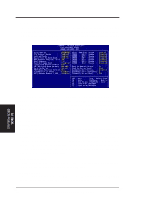
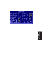
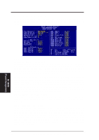
IV. BIOS (Chipset Features) (Chipset Features) IV. BIOS SOFTWARE [DRAM and ECC] If all your DRAM modules have parity chips (e.g. 8 chips + 4 parity chips), they are considered 36bits. This motherboard sums the memory per bank and therefore two modules will give 72bits and the following will be displayed: If your DRAM modules do not have parity chips (e.g. 8 chips), they are considered 32bits and the following will be displayed instead: The default of Disabled for Memory parity SERR# (NMI) will not show memory errors on your monitor. When using parity DRAM modules, you can select from the default of Parity or ECC (Error Checking and Correcting) to correct 1 bit memory errors that may occur in the memory. (See pages 12-13 for more information on DRAM memory modules.) ...Onboard FDC Controller When enabled, this field allows you to connect your floppy disk drives to the onboard floppy drive connector instead of a separate controller card. If you want to use a different controller card to connect the floppy drives, set this field to "Disabled". Default setting is Enabled. Onboard FDC Swap A: B: This field allows you to reverse the hardware drive letter assignments of your floppy disk drives. Two options are available: No Swap (default) and Swap AB. If you want to switch drive letter assignments through the onboard chipset, set this field to Swap AB. Onboard Serial Port 1 Settings are 3F8H/IRQ4 (default), 2F8H/IRQ3, 3E8H/IRQ4, 2E8H/IRQ10, and Disabled for the onboard serial connector. Onboard Serial Port 2 Settings are 3F8H/IRQ4, 2F8H/IRQ3 (default), 3E8H/IRQ4, 2E8H/IRQ10, and Disabled for the onboard serial connector. 38 ASUS P/I-P55T2P4 User's Manual
-
 1
1 -
2
-
3
-
4
-
5
-
6
-
7
-
8
-
9
-
10
-
11
-
12
-
13
-
14
-
15
-
16
-
17
-
18
-
19
-
20
-
21
-
22
-
23
-
24
-
25
-
26
-
27
-
28
-
29
-
30
-
31
-
32
-
33
-
34
-
35
-
36
-
37
-
38
-
 39
39 -
 40
40 -
 41
41 -
 42
42 -
 43
43 -
 44
44 -
 45
45 -
 46
46 -
 47
47 -
 48
48 -
 49
49 -
50
-
51
-
52
-
53
-
54
-
55
-
56
-
57
-
58
-
59
-
60
-
61
-
62
-
63
-
64
 |
 |