Biostar I915P-A7 I915P-A7 BIOS guide. - Page 16
Advanced Chipset Features
 |
View all Biostar I915P-A7 manuals
Add to My Manuals
Save this manual to your list of manuals |
Page 16 highlights
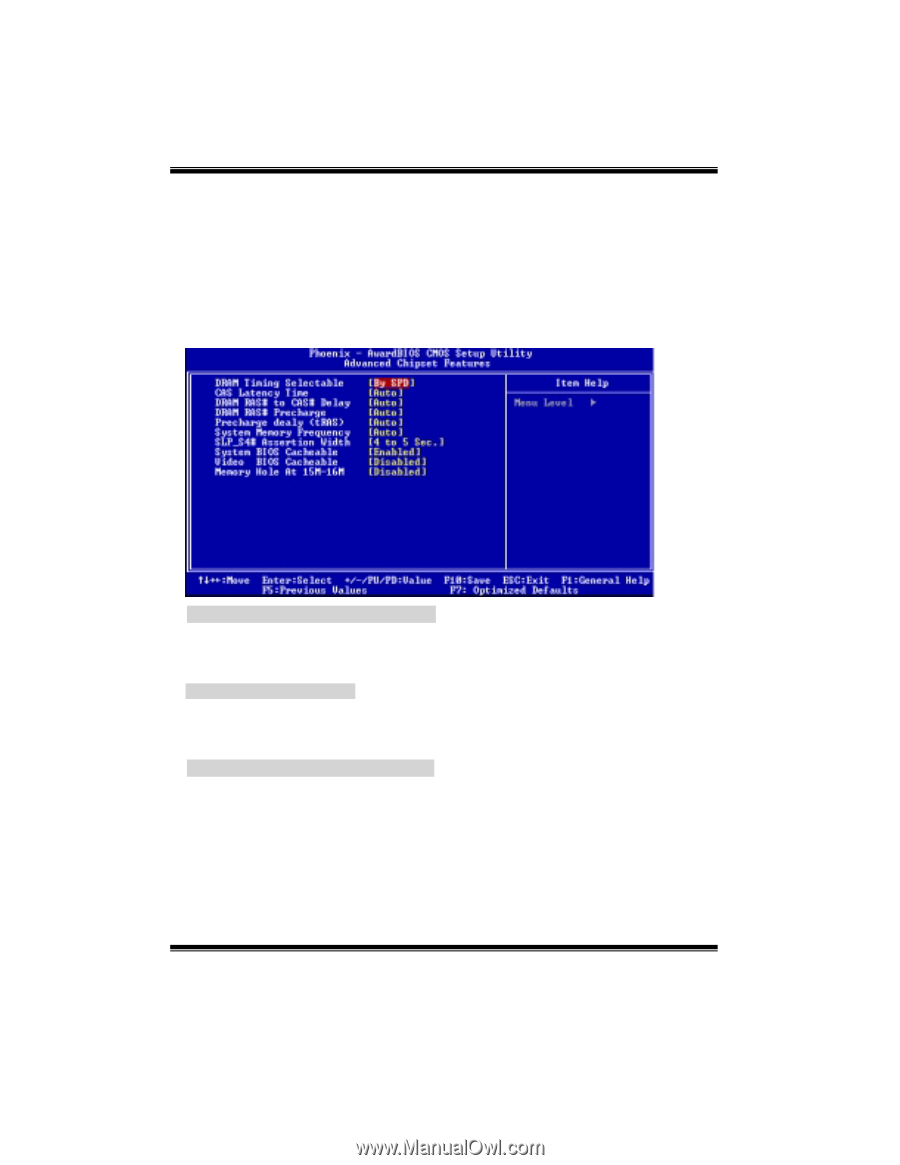
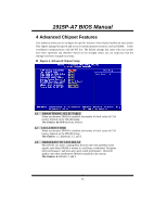
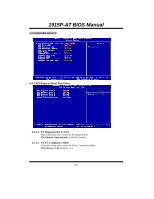
1915P-A7 BIOS Manual 4 Advanced Chipset Features This submenu allows you to configure the specific features of the chipset installed on your system. This chipset manage bus speeds and access to system memory resources, such as DRAM. It also coordinates communications with the PCI bus. The default settings that came with your system have been optimized and therefore should not be changed unless you are suspicious that the settings have been changed incorrectly. Figure 4. Advanced Chipset Setup 4.1 DRAM TIMING SELECTABLE When synchronous DRAM is installed, the number of clock cycles of CAS latency depends on the DRAM timing. The Choices: By SPD (default), Manual. 4.2 CAS LATENCY TIME When synchronous DRAM is installed, the number of clock cycles of CAS latency depends on the DRAM timing. The Choices: 1.5, 2(default), 2.5, and 3. 4.3 DRAM RAS# TO CAS# DELAY This field let you insert a timing delay between the CAS and RAS strobe signals, used when DRAM is written to, read from, or refreshed. Fast gives faster performance; and slow gives more stable performance. This field applies only when synchronous DRAM is installed in the system. The Choices: 4 (default), 3, and 2. 15
-
 1
1 -
2
-
3
-
4
-
5
-
6
-
7
-
8
-
9
-
10
-
 11
11 -
 12
12 -
 13
13 -
 14
14 -
 15
15 -
 16
16 -
 17
17 -
 18
18 -
 19
19 -
 20
20 -
 21
21 -
22
-
23
-
24
-
25
-
26
-
27
-
28
-
29
-
30
-
31
-
32
-
33
-
34
 |
 |