Biostar K8NHA GRAND K8NHA Grand BIOS setup guide - Page 15
CPU OverClock in MHz, AGP OverClock in MHz, AGP Aperture Size, AGP 3.0 Speed, AGP 2.0 Speed - specs
 |
View all Biostar K8NHA GRAND manuals
Add to My Manuals
Save this manual to your list of manuals |
Page 15 highlights
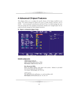
Write to Read Delay (tWTR) This bit specifies the write to read delay. Samsung called this Tcdlr (last data in to read command). It is measured from the rising edge following the last non-masked data strobe to the rising edge of the next Read Command (Jedec specs this as exactly one clock) The Choices: 1 BUS CLOCKS (Default), 2 BUS CLOCKS Read to Write Delay (tRWT) This bit specifies the Read to write delay. This is not a DRAM specified timing parameter but must be considered due to routing latencies on the clock forwarded bus. It is counted from first address bus slot which was not associated with part of the read burst. The Choices: 4 BUS CLOCKS (Default), 1 BUS CLOCKS, 2 BUS CLOCKS, 3 BUS CLOCKS, 5 BUS CLOCKS, 6 BUS CLOCKS. Refresh period (tREF) This field specifies the number of clock cycles between refresh. The Choices: 1x 2064 Cycles (Default). CPU OverClock in MHz The Choices: 200 (default), 201, 202, 203, 204, 205, 206, 207. AGP OverClock in MHz The Choices: 66 (default), 67, 68, 69, 70, 71, 72, 73. AGP Aperture Size Select the size of the Accelerated Graphics Port (AGP) aperture. The aperture is a portion of the PCI memory address range dedicated for graphics memory address space. Host cycles that hit the aperture range are forwarded to the AGP without any translation. The Choices: 64M, 256M, 128M (Default), 32M, 16M, 8M, 4M. AGP 3.0 Speed The Choices: Auto (default) AGP 2.0 Speed The Choices: Auto (default), 1x, 1x2x, 1x2x4x. AGP Fast Write 14
-
 1
1 -
2
-
3
-
4
-
5
-
6
-
7
-
8
-
9
-
 10
10 -
 11
11 -
 12
12 -
 13
13 -
 14
14 -
 15
15 -
 16
16 -
 17
17 -
 18
18 -
 19
19 -
 20
20 -
21
-
22
-
23
-
24
-
25
-
26
-
27
-
28
-
29
-
30
 |
 |
