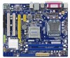
Foxconn G31MXP-K English Manual. - Page 38
DRAM Configuration
 |
View all Foxconn G31MXP-K manuals
Add to My Manuals
Save this manual to your list of manuals |
Page 38 highlights
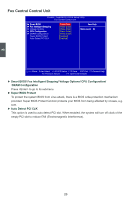
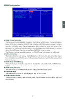
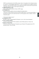
DRAM Configuration Phoenix - AwardBIOS CMOS Setup Utility DRAM Configuration DRAM Timing Selectable x CAS Latency Time x DRAM RAS# to CAS# Delay x DRAM RAS# Precharge x Precharge Delay x System Memory Speed [By SPD] Item Help Auto Auto Menu Level ► Auto Auto Auto 3 Move Enter:Select +/-/PU/PD:Value F10:Save ESC:Exit F1:General Help F5: Previous Values F7: Optimized Defaults ► DRAM Timing Selectable This item is used to enable/disable provision of DRAM timing by SPD device. The Serial Presence Detect (SPD) device is a small EEPROM chip, mounted on a DDR2 memory module. It contains important information about the module's speed, size, addressing mode and various other parameters, so that the motherboard memory controller (chipset) can better access the memory device. Select [Manual], then you can configure the DRAM timing manually. The following 5 settings are valid only when the DRAM Timing Selectable is set to [Manual]. ► CAS Latency Time This item controls the CAS latency. The CAS Latency is the number of clock cycles that elapse from the time the request for data is sent to the actual memory location until the data is transmitted from the module. ► DRAM RAS# to CAS# Delay This item allows you to select a delay time (in clock cycles) between the CAS and RAS strobe signals. ► DRAM RAS# Precharge This item allows you to select the DRAM RAS precharge time (in clock cycles). ► Precharge Delay This item allows you to set the precharge delay time (in clock cycles). ► System Memory Speed This item is used to manually select a DRAM speed. The options are [Auto], [533MHz], [667MHz] and [800MHz]. 31
-
 1
1 -
2
-
3
-
4
-
5
-
6
-
7
-
8
-
9
-
10
-
11
-
12
-
13
-
14
-
15
-
16
-
17
-
18
-
19
-
20
-
21
-
22
-
23
-
24
-
25
-
26
-
27
-
28
-
29
-
30
-
31
-
32
-
 33
33 -
 34
34 -
 35
35 -
 36
36 -
 37
37 -
 38
38 -
 39
39 -
 40
40 -
 41
41 -
 42
42 -
 43
43 -
44
-
45
-
46
-
47
-
48
-
49
-
50
-
51
-
52
-
53
-
54
-
55
-
56
-
57
-
58
-
59
-
60
-
61
-
62
-
63
-
64
-
65
-
66
-
67
-
68
-
69
-
70
-
71
-
72
-
73
-
74
-
75
-
76
-
77
-
78
 |
 |
