HP ML530 ProLiant ML530 High-Performance Technologies - Page 7
-MHz front side bus, This is accomplished with four overlapping clock strobes
 |
UPC - 720591250669
View all HP ML530 manuals
Add to My Manuals
Save this manual to your list of manuals |
Page 7 highlights
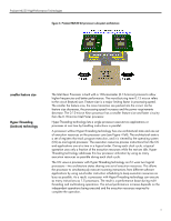
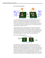
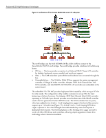
ProLiant ML530 High-Performance Technologies 400-MHz front side bus the Pentium III processor. As a result, there is greater chance of a cache hit for any given memory request. When a cache hit occurs in the L2 cache, the data is transferred at 2.8 GHz to the processor core along a 32-byte interface on each core clock cycle. As a result, the 512-kB L2 Advanced Transfer Cache can deliver a data transfer rate of 89.6 GB/s to the processor so that it can keep executing instructions instead of sitting idle. This compares to a transfer rate of 16 GB/s for the 1-GHz Intel® Pentium® III processor. If the requested information is not in L1 or L2 cache, the processor must issue a request to read it from the system memory. All data transfers go to and from the processor over the FSB. The Intel Xeon processor's FSB is a 64-bit, quad-pumped bus running at 100 MHz. A normal (single-pumped) bus sends, or latches, data out once per clock cycle on the rising or falling edge of the bus clock signal. A quad-pumped bus latches data at four times the rate of a normal bus (Figure 6). This is accomplished with four overlapping clock strobes, each operating 90 degrees out of phase with the next. Data is sent on the rising edge of each of the four strobes, four times per clock cycle. This makes it possible to transfer 3.2 GB/s of data on a 100-MHz FSB, which is triple the data rate of the Pentium III FSB (1.06 GB/s with a 133-MHz FSB). figure 6. comparison of clock signals for a quad-pumped and single pumped 100-MHz front side bus Note: Only the data is quad pumped on these buses. The address bus for the processor is double pumped. 7
-
 1
1 -
 2
2 -
 3
3 -
 4
4 -
 5
5 -
 6
6 -
 7
7 -
 8
8 -
 9
9 -
 10
10 -
 11
11 -
 12
12 -
13
-
14
 |
 |
