HP ProLiant DL280 Memory technology evolution: an overview of system memory te - Page 13
Prefetching, Double transition clocking
 |
View all HP ProLiant DL280 manuals
Add to My Manuals
Save this manual to your list of manuals |
Page 13 highlights
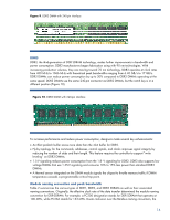
data bus, and Stub-Series Terminated Logic_2 (SSTL_2) low-voltage signaling. At 400 MHz, DDR increases memory bandwidth to 3.2 GB/s-400% more than original SDRAM. Prefetching SDRAM transfers one bit per clock cycle from the memory cell array to the I/O buffer or data queue (DQ). The I/O buffer releases one bit to the bus per pin and clock cycle (on the rising edge of the clock signal). To double the data rate, DDR SDRAM uses a technique called prefetching to transfer two bits from the memory cell array to the I/O buffer in two separate pipelines. Then the I/O buffer releases the bits in the order of the queue on the same output line. This is a 2n-prefetch architecture because the DRAM fetches two data bits from the memory cell array before releasing them to the bus in a time-multiplexed manner. Double transition clocking Standard DRAM transfers one data bit to the bus on the rising edge of the bus clock signal, while DDR1 uses both the rising and falling edges of the clock to trigger the data transfer to the bus. This technique, known as double transition clocking, delivers twice the bandwidth of SDRAM without increasing the clock frequency. DDR1 has theoretical peak data transfer rates of 1.6 and 2.1 GB/s at clock frequencies of 100 MHz and 133 MHz, respectively. Stub-Series Terminated Logic_2 (SSTL_2) low-voltage signaling technology The signaling technology is another difference between SDRAM and DDR1. Instead of using a 3.3-V operating voltage of SDRAM, DDR1 uses the 2.5-V signaling specification SSTL_2. This low-voltage signaling results in lower power consumption and improved heat dissipation. Strobe-based data bus SSTL_2 signaling lets DDR1 run faster than traditional SDRAM. DDR1 also uses a delay-locked loop (one for every 16 outputs) to provide a data strobe signal as data becomes valid on the SDRAM pins. The memory controller uses the data strobe signal to locate data more accurately and resynchronize incoming data from different DIMMs. DDR1 operates at transfer rates of 400 Mb/s, or 3.2 GB/s. Although the data bus is capable of running at these speeds, the command bus cannot. The use of strobes alleviated tight system timing requirements on the data bus. But the command bus does not use a strobe and must still meet setup times to a synchronous clock, so at a data rate of 400 Mb/s, the command bus must operate at 200 MHz. DDR1 DIMMs DDR1 DIMMs require 184 pins instead of the 168 pins used by standard SDRAM DIMMs. DDR1 is versatile enough for both desktop PCs and servers. To vary the cost of DDR1 DIMMs for these different markets, memory manufacturers offer unbuffered and registered versions. Unbuffered DDR1 DIMMs place the load of all the DDR modules on the system memory bus. Use Unbuffered DIMMS in systems that do not require high memory capacity. On the other hand, registered DDR1 DIMMs place only one load per DIMM on the memory bus, regardless of how many SDRAM devices are on the module. They are best suited for servers with high memory capacities. DDR2 DDR2 is the second generation of DDR SDRAM technology. It provides data rates of up to 6.4 GB/s, lower power consumption, and improvements in packaging. At 400 MHz and 800 Mb/s, DDR2 increases memory bandwidth to 6.4 GB/s-800% more than original SDRAM. DDR2 SDRAM achieves higher performance level and lower power consumption through faster clocks, 1.8-V operation and signaling, along with a simplified command set. The 240-pin connector on DDR2 accommodates differential strobe signals (Figure 9). 13
-
 1
1 -
2
-
3
-
4
-
5
-
6
-
7
-
 8
8 -
 9
9 -
 10
10 -
 11
11 -
 12
12 -
 13
13 -
 14
14 -
 15
15 -
 16
16 -
 17
17 -
 18
18 -
19
 |
 |
