HP ProLiant DL280 Memory technology evolution: an overview of system memory te - Page 3
These actions are Row Address Strobe RAS and Column Address Strobe CAS. The Write
 |
View all HP ProLiant DL280 manuals
Add to My Manuals
Save this manual to your list of manuals |
Page 3 highlights
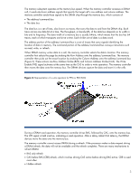
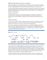
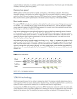
The memory subsystem operates at the memory bus speed. When the memory controller accesses a DRAM cell, it sends electronic address signals that specify the target cell's row address and column address. The memory controller sends these signals to the DRAM chip through the memory bus, which consists of: • The address/command bus • The data bus The data bus is a set of lines, also known as traces, that carry the data to and from the DRAM chip. Each trace carries one data bit at a time. The throughput, or bandwidth, of the data bus depends on its width in bits and its frequency. The data width of a memory bus is usually 64-bits, which means that the bus has 64 traces, each of which transports one bit at a time. Each 64-bit unit of data is a data word. The address portion of the address/command bus is a set of traces that carry signals identifying the location of data in memory. The command portion of the address/command bus conveys instructions such as read, write, or refresh. When DRAM memory writes data to a cell, the memory controller selects the data's location. The memory controller first selects the page by strobing the Row Address onto the address/command bus. The memory controller then picks out the exact location by strobing the Column Address onto the address/command bus (Figure 2). These actions are Row Address Strobe (RAS) and Column Address Strobe (CAS). The Write Enable (WE) signal activates at the same time as the CAS to order a write operation. The memory controller then moves the data onto the memory bus. The DRAM devices capture the data and store it in the cells. Figure 2. Representation of a write operation for FPM or EDO RAM During a DRAM read operation, the memory controller drives RAS, followed by CAS, onto the memory bus. The WE signal is held inactive, indicating a read operation. After a delay called CAS Latency, the DRAM devices move the data onto the memory bus. The memory controller cannot access DRAM during a refresh. If the processor makes a data request during a DRAM refresh, the data will not be available until the refresh completes. There are many mechanisms to refresh DRAM: • RAS only refresh • CAS before RAS (CBR) refresh, which involves driving CAS active before driving RAS active. CBR is used most often • Hidden refresh 3
-
 1
1 -
 2
2 -
 3
3 -
 4
4 -
 5
5 -
 6
6 -
 7
7 -
 8
8 -
 9
9 -
10
-
11
-
12
-
13
-
14
-
15
-
16
-
17
-
18
-
19
 |
 |
