HP Professional 8000 Highly Parallel System Architecture for Compaq Profession - Page 5
Dual Memory Buses, Column Address Strobe CAS precharge.
 |
View all HP Professional 8000 manuals
Add to My Manuals
Save this manual to your list of manuals |
Page 5 highlights
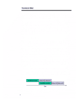
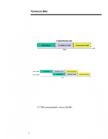
ECG066/1198 TECHNOLOGY BRIEF (cont.) ... up to 16 instructions. Because multimedia operations such as video and audio use a number of redundant instructions, MMX achieves some efficiencies by using a technique called SIMD (single instruction multiple data). SIMD reduces the required number of clock cycles by performing redundant instructions on multiple sets of data. For its L2 cache, the Pentium II processor uses industry-standard SRAM (static random access memory). This implementation is sometimes referred to as a half-speed cache because the SRAM runs at half the core processor speed. Use of a half-speed L2 cache instead of a full-speed L2 cache improves manufacturability; however, it increases cache access time, which limits scalability and performance. Pentium II systems will support a maximum of two processors and are limited to 512 MB of addressable system memory. The Pentium II processor is capable of caching 512 MB of system memory. Adding more memory will significantly degrade system performance because the additional memory will not be cached. Therefore, to ensure application performance, the Compaq Professional Workstation 6000 will not boot if more than 512 MB of system memory is installed. DUAL MEMORY BUSES The new architecture also includes two independently operating memory buses, each running at a peak speed of 533 MB/s. Together they provide a peak aggregate memory bandwidth of 1.07 GB/s-two to four times the memory bandwidth of other X86/NT workstations. This high memory bandwidth is the key to delivering the highest performance levels of both single processor and SMP-aware applications. Each memory bus is 144 bits wide and consists of 128 bits of data plus 16 bits for Error Checking and Correction (ECC). The new architecture uses buffered 60-ns Extended Data Out (EDO) DIMMs (Dual Inline Memory Modules), and the memory is interleaved. Interleaved memory takes advantage of the sequential nature of program execution to overcome delays resulting from Column Address Strobe (CAS) precharge. CAS precharge is the time a microprocessor must wait between back-to-back accesses to the same Dynamic Random Access Memory (DRAM) chip while the DRAM chip charges back up after a destructive read. When interleaved memory is used, banks of DRAM are divided into two or more physically separate areas. Consecutive addresses are stored in different areas of a bank. This makes it possible for the next sequential read to begin on bank B while bank A is precharging from the previous read, and vice versa. Thus, interleaved memory can significantly increase memory throughput for sequential reads. EDO memory is capable of transferring data every other clock cycle (30 ns for a 60-MHz bus). Non-EDO (Fast Page Mode) memory, on the other hand, is capable of transferring data every four clocks (60 ns for a 66-MHz bus). With the combination of interleaved memory and EDO memory, 128 bits of data (plus 16 bits ECC) are read at a time. As Figure 2 illustrates, the first 64 bits of the read go to the processor on one clock pulse, and the second 64 bits of data go on the next clock pulse. This enables the memory bus to transfer data at the peak data rate of the processor. Read 128 bits from RAM 64 bits to CPU 64 bits to CPU Read 128 bits from RAM 64 bits to CPU 64 bits to CPU Time Figure 2. Interleaved EDO memory reads 128 data bits at a time and transfers data every other clock cycle. 5
-
 1
1 -
 2
2 -
 3
3 -
 4
4 -
 5
5 -
 6
6 -
 7
7 -
 8
8 -
 9
9 -
 10
10 -
 11
11 -
12
-
13
 |
 |