Intel 521 Data Sheet - Page 22
GTL+ Asynchronous Signals
 |
UPC - 683728199029
View all Intel 521 manuals
Add to My Manuals
Save this manual to your list of manuals |
Page 22 highlights
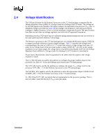
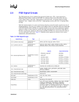
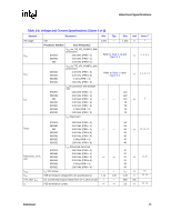
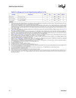
Electrical Specifications NOTES: 1. Refer to Section 4.2 for signal descriptions. 2. In processor systems where there is no debug port implemented on the system board, these signals are used to support a debug port interposer. In systems with the debug port implemented on the system board, these signals are no connects. 3. The value of these signals during the active-to-inactive edge of RESET# defines the processor configuration options. See Section 6.1 for details. Table 2-4. Signal Characteristics Signals with RTT A[35:3]#, ADS#, ADSTB[1:0]#, AP[1:0]#, BINIT#, BNR#, BOOTSELECT1, BPRI#, D[63:0]#, DBI[3:0]#, DBSY#, DEFER#, DP[3:0]#, DRDY#, DSTBN[3:0]#, DSTBP[3:0]#, HIT#, HITM#, LOCK#, MCERR#, PROCHOT#, REQ[4:0]#, RS[2:0]#, RSP#, TRDY# Open Drain Signals2 Signals with no RTT A20M#, BCLK[1:0], BPM[5:0]#, BR0#, BSEL[2:0], COMP[1:0], FERR#/PBE#, IERR#, IGNNE#, INIT#, LINT0/INTR, LINT1/NMI, PWRGOOD, RESET#, SKTOCC#, SMI#, STPCLK#, TDO, TESTHI[13:0], THERMDA, THERMDC, THERMTRIP#, VID[5:0], VTTPWRGD, GTLREF, TCK, TDI, TRST#, TMS BSEL[2:0], VID[5:0], THERMTRIP#, FERR#/PBE#, IERR#, BPM[5:0]#, BR0#, TDO, VTT_SEL, LL_ID[1:0], MSID[1:0] NOTES: 1. The BOOTSELECT signal has a 500-5000 Ω pull-up to VTT rather than on-die termination. 2. Signals that do not have RTT, nor are actively driven to their high-voltage level. . Table 2-5. Signal Reference Voltages GTLREF VTT/2 BPM[5:0]#, LINT0/INTR, LINT1/NMI, RESET#, BINIT#, BNR#, HIT#, HITM#, MCERR#, PROCHOT#, BR0#, A[35:0]#, ADS#, ADSTB[1:0]#, AP[1:0]#, BPRI#, D[63:0]#, DBI[3:0]#, DBSY#, DEFER#, DP[3:0]#, DRDY#, DSTBN[3:0]#, DSTBP[3:0]#, LOCK#, REQ[4:0]#, RS[2:0]#, RSP#, TRDY# BOOTSELECT, VTTPWRGD, A20M#, IGNNE#, INIT#, PWRGOOD1, SMI#, STPCLK#, TCK1, TDI1, TMS1, TRST#1 NOTES: 1. These signals also have hysteresis added to the reference voltage. See Table 2-13 for more information. 2.7 GTL+ Asynchronous Signals Legacy input signals such as A20M#, IGNNE#, INIT#, SMI#, and STPCLK# use CMOS input buffers. All of these signals follow the same DC requirements as GTL+ signals, however the outputs are not actively driven high (during a logical 0 to 1 transition) by the processor. These signals do not have setup or hold time specifications in relation to BCLK[1:0]. All of the GTL+ Asynchronous signals are required to be asserted/de-asserted for at least six BCLKs for the processor to recognize the proper signal state. See Section 6.2 for additional timing requirements for entering and leaving the low power states. 22 Datasheet
-
 1
1 -
2
-
3
-
4
-
5
-
6
-
7
-
8
-
9
-
10
-
11
-
12
-
13
-
14
-
15
-
16
-
 17
17 -
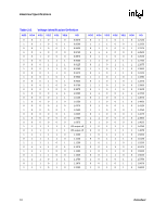 18
18 -
 19
19 -
 20
20 -
 21
21 -
 22
22 -
 23
23 -
 24
24 -
 25
25 -
 26
26 -
 27
27 -
28
-
29
-
30
-
31
-
32
-
33
-
34
-
35
-
36
-
37
-
38
-
39
-
40
-
41
-
42
-
43
-
44
-
45
-
46
-
47
-
48
-
49
-
50
-
51
-
52
-
53
-
54
-
55
-
56
-
57
-
58
-
59
-
60
-
61
-
62
-
63
-
64
-
65
-
66
-
67
-
68
-
69
-
70
-
71
-
72
-
73
-
74
-
75
-
76
-
77
-
78
-
79
-
80
-
81
-
82
-
83
-
84
-
85
-
86
-
87
-
88
-
89
-
90
-
91
-
92
-
93
-
94
-
95
-
96
 |
 |