Intel SL3VS Specification Update - Page 88

C3., Direction Flag (DF) Mistakenly Denoted as a System Flag, C4., Fopcode Compatibility Mode

Page 88 highlights

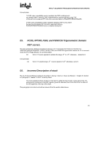
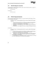
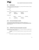
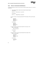
INTEL® CELERON® PROCESSOR SPECIFICATION UPDATE C2. Executing the SSE2 Variant on a Non-SSE2 Capable Processor In Intel Architecture Software Developer's Manual, Vol 2: Instruction Set Reference the section for each of the following instructions states that executing the instruction in real or protected mode on a processor for which the SSE2 feature flag returned by CPUID is 0 (SSE2 not supported by the processor) will result in the generation of an undefined opcode exception (#UD). This is incorrect. The SSE2 form of these instructions is defined by opcodes for which the leading opcode byte maps into an operand size prefix. Executing the SSE2 variant of these instructions on a non-SSE2 capable processor will result in an SSE like operation and not a #UD. Refer to section 2.2 of the Intel Architecture Software Developer's Manual, Vol 2 for more detail. Instructions: MOVD xmm, r32; MOVD r32, xmm; MOVDQA; MOVDQU; MOVQ xmm, m64; PACKSSWB/DW; PACKUSWB; PADDB/W/D; PADDSB/W; PADDUSB/W; PAND; PANDN; PCMPEQB/W/D; PCMPGTB/W/D; PMADDWD; PMULHW; PMULLW; POR; PSLLW/D/Q; PSRAW/D; PSRLW/D/Q; PSUBB/W/D; PSUBSB/W; PSUBUSB/W; PUNPCKHBW/WD/DQ; PUNPCKLBW/WD/DQ; PXOR. C3. Direction Flag (DF) Mistakenly Denoted as a System Flag The Intel Architecture Software Developer's Manual, Vol 1: Basic Architecture Section 3.4.3 "EFLAGS Register", in Figure 3-7. EFLAGS Register currently states: X Direction Flag(DF) It should state: C Direction Flag(DF) C4. Fopcode Compatibility Mode The Intel Architecture Software Developer's Manual, Vol 1: Basic Architecture Section 8.1.8.1 "FOPCODE COMPATIBILITY MODE" currently states: "When the FOP code compatibility mode is enabled, the IA32 architecture guarantees that if an unmasked x87 FPU floating-point exception is generated, the opcode of the last non-control instruction executed prior to the generation of the exception will be stored in the x87 FPU opcode register, and that value can be read by a subsequent FSAVE of FXSAVE instruction. When the fop compatibility mode is disabled (default), the value stored in the x87 FPU opcode register is undefined (reserved)." 80

  • 1
  • 2
  • 3
  • 4
  • 5
  • 6
  • 7
  • 8
  • 9
  • 10
  • 11
  • 12
  • 13
  • 14
  • 15
  • 16
  • 17
  • 18
  • 19
  • 20
  • 21
  • 22
  • 23
  • 24
  • 25
  • 26
  • 27
  • 28
  • 29
  • 30
  • 31
  • 32
  • 33
  • 34
  • 35
  • 36
  • 37
  • 38
  • 39
  • 40
  • 41
  • 42
  • 43
  • 44
  • 45
  • 46
  • 47
  • 48
  • 49
  • 50
  • 51
  • 52
  • 53
  • 54
  • 55
  • 56
  • 57
  • 58
  • 59
  • 60
  • 61
  • 62
  • 63
  • 64
  • 65
  • 66
  • 67
  • 68
  • 69
  • 70
  • 71
  • 72
  • 73
  • 74
  • 75
  • 76
  • 77
  • 78
  • 79
  • 80
  • 81
  • 82
  • 83
  • 84
  • 85
  • 86
  • 87
  • 88
  • 89
  • 90
  • 91
  • 92
  • 93
  • 94
  • 95
  • 96
  • 97
  • 98
  • 99
  • 100
  • 101
  • 102
  • 103
  • 104
  • 105
  • 106
  • 107
  • 108

INTEL
®
CELERON® PROCESSOR SPECIFICATION UPDATE
80
C2.
Executing the SSE2 Variant on a Non-SSE2 Capable
Processor
In
Intel Architecture Software Developer's Manual, Vol 2
:
Instruction Set Reference
the section for each of the
following instructions states that executing the instruction in real or protected mode on a processor for which
the SSE2 feature flag returned by CPUID is 0 (SSE2 not supported by the processor) will result in the
generation of an undefined opcode exception (#UD). This is incorrect. The SSE2 form of these instructions is
defined by opcodes for which the leading opcode byte maps into an operand size prefix. Executing the SSE2
variant of these instructions on a non-SSE2 capable processor will result in an SSE like operation and not a
#UD. Refer to section 2.2 of the
Intel Architecture Software Developer's Manual, Vol 2
for more detail.
Instructions:
MOVD xmm, r32; MOVD r32, xmm; MOVDQA; MOVDQU; MOVQ xmm, m64; PACKSSWB/DW;
PACKUSWB; PADDB/W/D; PADDSB/W; PADDUSB/W; PAND; PANDN; PCMPEQB/W/D; PCMPGTB/W/D;
PMADDWD; PMULHW; PMULLW; POR; PSLLW/D/Q; PSRAW/D; PSRLW/D/Q; PSUBB/W/D; PSUBSB/W;
PSUBUSB/W; PUNPCKHBW/WD/DQ; PUNPCKLBW/WD/DQ; PXOR.
The
Intel Architecture Software Developer's Manual, Vol 1: Basic Architecture
Section 3.4.3 "EFLAGS
Register", in Figure 3-7. EFLAGS Register currently states:
X Direction Flag(DF)
It should state:
C Direction Flag(DF)
The
Intel Architecture Software Developer's Manual, Vol 1: Basic Architecture
Section 8.1.8.1 "FOPCODE
COMPATIBILITY MODE" currently states:
"When the FOP code compatibility mode is enabled, the IA32 architecture
guarantees that if an unmasked x87 FPU floating-point exception is generated, the opcode of the
last non-control instruction executed prior to the generation of the exception will be stored in the x87
FPU opcode register, and that value can be read by a subsequent FSAVE of FXSAVE instruction.
When the fop compatibility mode is disabled (default), the value stored in the x87 FPU opcode
register is undefined (reserved)."
C3.
Direction Flag (DF) Mistakenly Denoted as a System Flag
C4.
Fopcode Compatibility Mode