LG KE600 Service Manual - Page 67
Dual Mode Operation, 26.1 PAM Schematic
 |
View all LG KE600 manuals
Add to My Manuals
Save this manual to your list of manuals |
Page 67 highlights
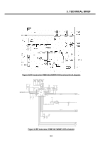
3. TECHNICAL BRIEF Table 13 PAM pin description PIN Function Description 1 HB_RFIN RF input to the High-band PA 2 BAND_SEL Logic low=low band, Logic high=high band select 3 TX_EN PA Enable 4 VBATT Main supply 5 VMODE Logic low=GMSK mode, Logic high=8PSK mode select 6 VRAMP Ramped burst pin 7 LB_RFIN RF input to the Low-band PA 8,9,10,11 GND Ground 12 LB_ RFOUT RF output from the low-band PA 13,14,15,16,17 GND 18 HB_RFOUT RF output from the high-band PA 19,20,21,22,23 GND Table 13 PAM pin description 3.26. Dual Mode Operation MODE GSM EDGE VMODE Low High RF INPUT Fixed Ramp Burst Control VRAMP Ramp Burst Control Control amp bias current TX ENABLE High High When VMODE is low, the voltage on VRAMP is used to regulate the PA collector voltage which directly controls the output power. When VMODE is high, the PA collector voltage is regulated to 3.6V, and the supply for the PA base bias can be adjusted via the VRAMP pin to optimize current drain for low or high power ranges. In addition, in 8PSK mode, the first stage of the low band PA is bypassed to decrease gain, but in high band, the PA operates with all stages. 3.26.1 PAM Schematic GND11 23 GND10 22 GND9 21 GND8 19 GND7 GND6 17 GND5 16 GND4 14 GND3 13 GND2 11 9 GND1 8 C640 4.7p L605 15nH L601 3.9nH L606 22nH C611 0.5p C612 0.5p NC3 20 15 NC2 10 NC1 12 LB_RFOUT HB_RFOUT 18 RF3158 LB_RFIN 7 VRAMP 6 VMODE 5 VBATT 4 TX_EN 3 BAND_SEL 2 HB_RFIN 1 U601 VSUPPLY C638 3p C639 C620 10p 56p C621 18p C613 68u LBAND_PAM_IN R611 15K HBAND_PAM_IN R612 R613 R614 100K 100K 100K PA_LEVEL MODE TXON_PA PA_BAND Figure 42 PAM schematic - 68 -
-
 1
1 -
2
-
3
-
4
-
5
-
6
-
7
-
8
-
9
-
10
-
11
-
12
-
13
-
14
-
15
-
16
-
17
-
18
-
19
-
20
-
21
-
22
-
23
-
24
-
25
-
26
-
27
-
28
-
29
-
30
-
31
-
32
-
33
-
34
-
35
-
36
-
37
-
38
-
39
-
40
-
41
-
42
-
43
-
44
-
45
-
46
-
47
-
48
-
49
-
50
-
51
-
52
-
53
-
54
-
55
-
56
-
57
-
58
-
59
-
60
-
61
-
 62
62 -
 63
63 -
 64
64 -
 65
65 -
 66
66 -
 67
67 -
 68
68 -
 69
69 -
 70
70 -
 71
71 -
 72
72 -
73
-
74
-
75
-
76
-
77
-
78
-
79
-
80
-
81
-
82
-
83
-
84
-
85
-
86
-
87
-
88
-
89
-
90
-
91
-
92
-
93
-
94
-
95
-
96
-
97
-
98
-
99
-
100
-
101
-
102
-
103
-
104
-
105
-
106
-
107
-
108
-
109
-
110
-
111
-
112
-
113
-
114
-
115
-
116
-
117
-
118
-
119
-
120
-
121
-
122
-
123
-
124
-
125
-
126
-
127
-
128
-
129
-
130
-
131
-
132
-
133
-
134
-
135
-
136
-
137
-
138
-
139
-
140
-
141
-
142
-
143
-
144
-
145
-
146
-
147
-
148
-
149
-
150
-
151
-
152
-
153
-
154
-
155
-
156
-
157
-
158
-
159
-
160
-
161
-
162
-
163
-
164
-
165
-
166
-
167
-
168
 |
 |
