MSI 760GME51 User Guide - Page 61
Onboard VGA Core Overclock
 |
View all MSI 760GME51 manuals
Add to My Manuals
Save this manual to your list of manuals |
Page 61 highlights
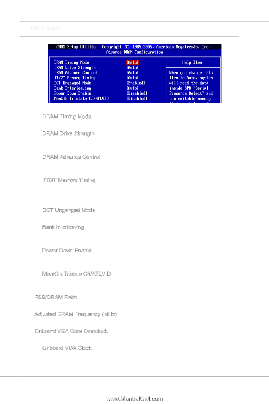
▍ BIOS Setup ▶ DRAM Timing Mode This field has the capacity to automatically detect all of the DRAM timing. ▶ DRAM Drive Strength This item allows you to control the memory data bus' signal strength. Increasing the drive strength of the memory bus can increase stability during overclocking. ▶ DRAM Advance Control This field has the capacity to automatically detect the advanced DRAM timing. If you set this field to [DCT 0], [DCT 1] or [Both], some fields will appear and selectable. ▶ 1T/2T Memory Timing This item controls the SDRAM command rate. Select [1T] makes SDRAM signal controller to run at 1T (T=clock cycles) rate. Selecting [2T] makes SDRAM signal controller run at 2T rate. ▶ DCT Unganged Mode This feature is used to Integrate two 64-bit DCTs into a 128-bit interface. ▶ Bank Interleaving Bank Interleaving is an important parameter for improving overclocking capability of memory. It allows system to access multiple banks simultaneously. ▶ Power Down Enable This is a memory power-saving technology. When the system does not access memory over a period of time, it will automatically reduce the memory power supply. ▶ MemClk Tristate C3/ATLVID This setting allows you to enable/disable the MemClk Tristating during C3 and ATLVID. ▶ FSB/DRAM Ratio This item allows you to select the ratio of FSB/ DRAM. ▶ Adjusted DRAM Frequency (MHz) It shows the adjusted Memory frequency. Read-only. ▶ Onboard VGA Core Overclock This item allows you to overclock the onboard VGA. ▶ Onboard VGA Clock This item will appear when Onboard VGA Over Clock sets to [Enabled]. It allows you to adjust the onboard VGA clock. 3-22
-
 1
1 -
2
-
3
-
4
-
5
-
6
-
7
-
8
-
9
-
10
-
11
-
12
-
13
-
14
-
15
-
16
-
17
-
18
-
19
-
20
-
21
-
22
-
23
-
24
-
25
-
26
-
27
-
28
-
29
-
30
-
31
-
32
-
33
-
34
-
35
-
36
-
37
-
38
-
39
-
40
-
41
-
42
-
43
-
44
-
45
-
46
-
47
-
48
-
49
-
50
-
51
-
52
-
53
-
54
-
55
-
 56
56 -
 57
57 -
 58
58 -
 59
59 -
 60
60 -
 61
61 -
 62
62 -
 63
63 -
 64
64 -
 65
65 -
 66
66 -
67
-
68
-
69
-
70
-
71
-
72
-
73
-
74
-
75
-
76
-
77
-
78
-
79
-
80
-
81
-
82
-
83
-
84
-
85
-
86
-
87
-
88
-
89
-
90
-
91
-
92
-
93
-
94
-
95
-
96
-
97
-
98
-
99
-
100
-
101
-
102
-
103
-
104
-
105
-
106
 |
 |