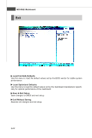
MSI Fuzzy User Guide - Page 63
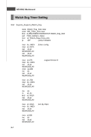
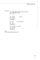
Check Point List, POST hex, Description
 |
View all MSI Fuzzy manuals
Add to My Manuals
Save this manual to your list of manuals |
Page 63 highlights
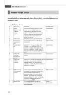
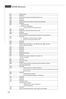
System Resources · Check Point List POST (hex) Description CFh Test CMOS R/W functionality. C0h Early chipset initialization: -Disable shadow RAM -Disable L2 cache (socket 7 or below) -Program basic chipset registers C1h Detect memory -Auto-detection of DRAM size, type and ECC. -Auto-detection of L2 cache (socket 7 or below) A1h Set Initial Conditions (Default Values) in EBP A2h Determine FSB frequency. A3h Begin Detection of installed DIMMS A4h Check for Column Latency A5h 200Mhz or 266Mhz A6h Check for tRAS timing A7h Check for tRP timing A8h Check for tRCD timing A9h Check for ECC Support AAh Check for refresh timing ABh Verify that the DIMM's are in matched pairs C3h Expand compressed BIOS code to DRAM C5h Call chipset hook to copy BIOS back to E000 & F000 shadow RAM. 01h Expand the Xgroup codes locating in physical address 1000:0 02h Reserved 03h Initial Superio_Early_Init switch. 04h Reserved 05h 1. Blank out screen 2. Clear CMOS error flag 06h Reserved 07h 1. Clear 8042 interface 2. Initialize 8042 self-test 08h 1. Test special keyboard controller for Winbond 977 series Super I/O chips. 2. Enable keyboard interface. 09h Reserved 0Ah 1. Disable PS/2 mouse interface (optional). 2. Auto detect ports for keyboard & mouse followed by a port & interface swap (optional). 3. Reset keyboard for Winbond 977 series Super I/O chips. 0Bh Reserved 0Ch Reserved 0Dh Reserved 0Eh Test F000h segment shadow to see whether it is R/W-able or not. If test fails, keep beeping the speaker. 0Fh Reserved 4-5
-
 1
1 -
2
-
3
-
4
-
5
-
6
-
7
-
8
-
9
-
10
-
11
-
12
-
13
-
14
-
15
-
16
-
17
-
18
-
19
-
20
-
21
-
22
-
23
-
24
-
25
-
26
-
27
-
28
-
29
-
30
-
31
-
32
-
33
-
34
-
35
-
36
-
37
-
38
-
39
-
40
-
41
-
42
-
43
-
44
-
45
-
46
-
47
-
48
-
49
-
50
-
51
-
52
-
53
-
54
-
55
-
56
-
57
-
 58
58 -
 59
59 -
 60
60 -
 61
61 -
 62
62 -
 63
63 -
 64
64 -
 65
65 -
 66
66 -
 67
67 -
 68
68 -
69
-
70
-
71
-
72
-
73
-
74
-
75
-
76
-
77
-
78
 |
 |
