MSI Fuzzy User Guide - Page 68
Check Point & Beep Code List
 |
View all MSI Fuzzy manuals
Add to My Manuals
Save this manual to your list of manuals |
Page 68 highlights
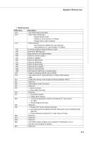
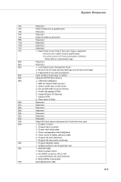
MS-9642 Mainboard Check Point & Beep Code List Bootblock Initialization Code Checkpoints Checkpoint Description Before D0 If boot block debugger is enabled, CPU cache-as-RAM functionality is enabled at this point. Stack will be enabled from this point. D0 Early Boot Strap Processor (BSP) initialization like microcode update, frequency and other CPU critical initialization. Early chipset initialization is done. D1 Early super I/O initialization is done including RTC and keyboard controller. Serial port is enabled at this point if needed for debugging. NMI is disabled. Perform keyboard controller BAT test. Save power-on CPUID value in scratch CMOS. Go to flat mode with 4GB limit and GA20 enabled. D2 Verify the boot block checksum. System will hang here if checksum is bad. D3 Disable CACHE before memory detection. Execute full memory sizing module. If memory sizing module not executed, start memory refresh and do memory sizing in Boot block code. Do additional chipset initialization. Re-enable CACHE. Verify that flat mode is enabled. D4 Test base 512KB memory. Adjust policies and cache first 8MB. Set stack. D5 Bootblock code is copied from ROM to lower system memory and control is given to it. BIOS now executes out of RAM. Copies compressed boot block code to memory in right segments. Copies BIOS from ROM to RAM for faster access. Performs main BIOS checksum and updates recovery status accordingly. D6 Both key sequence and OEM specific method is checked to determine if BIOS recovery is forced. If BIOS recovery is necessary, control flows to checkpoint E0. See Bootblock Recovery Code Checkpoints section of document for more information. D7 Restore CPUID value back into register. The Bootblock-Runtime interface module is moved to system memory and control is given to it. Determine whether to execute serial flash. D8 D9 DA DC E1-E8 EC-EE The Runtime module is uncompressed into memory. CPUID information is stored in memory. Store the Uncompressed pointer for future use in PMM. Copying Main BIOS into memory. Leaves all RAM below 1MB Read-Write including E000 and F000 shadow areas but closing SMRAM. Restore CPUID value back into register. Give control to BIOS POST (ExecutePOSTKernel). See POST Code Checkpoints section of document for more information. System is waking from ACPI S3 state OEM memory detection/configuration error. This range is reserved for chipset vendors & system manufacturers. The error associated with this value may be different from one platform to the next. 4-10
-
 1
1 -
2
-
3
-
4
-
5
-
6
-
7
-
8
-
9
-
10
-
11
-
12
-
13
-
14
-
15
-
16
-
17
-
18
-
19
-
20
-
21
-
22
-
23
-
24
-
25
-
26
-
27
-
28
-
29
-
30
-
31
-
32
-
33
-
34
-
35
-
36
-
37
-
38
-
39
-
40
-
41
-
42
-
43
-
44
-
45
-
46
-
47
-
48
-
49
-
50
-
51
-
52
-
53
-
54
-
55
-
56
-
57
-
58
-
59
-
60
-
61
-
62
-
 63
63 -
 64
64 -
 65
65 -
 66
66 -
 67
67 -
 68
68 -
 69
69 -
 70
70 -
 71
71 -
 72
72 -
 73
73 -
74
-
75
-
76
-
77
-
78
 |
 |
