MSI K9AGM2-FIH User Guide - Page 47
Advanced Chipset Features
 |
UPC - 816909038378
View all MSI K9AGM2-FIH manuals
Add to My Manuals
Save this manual to your list of manuals |
Page 47 highlights
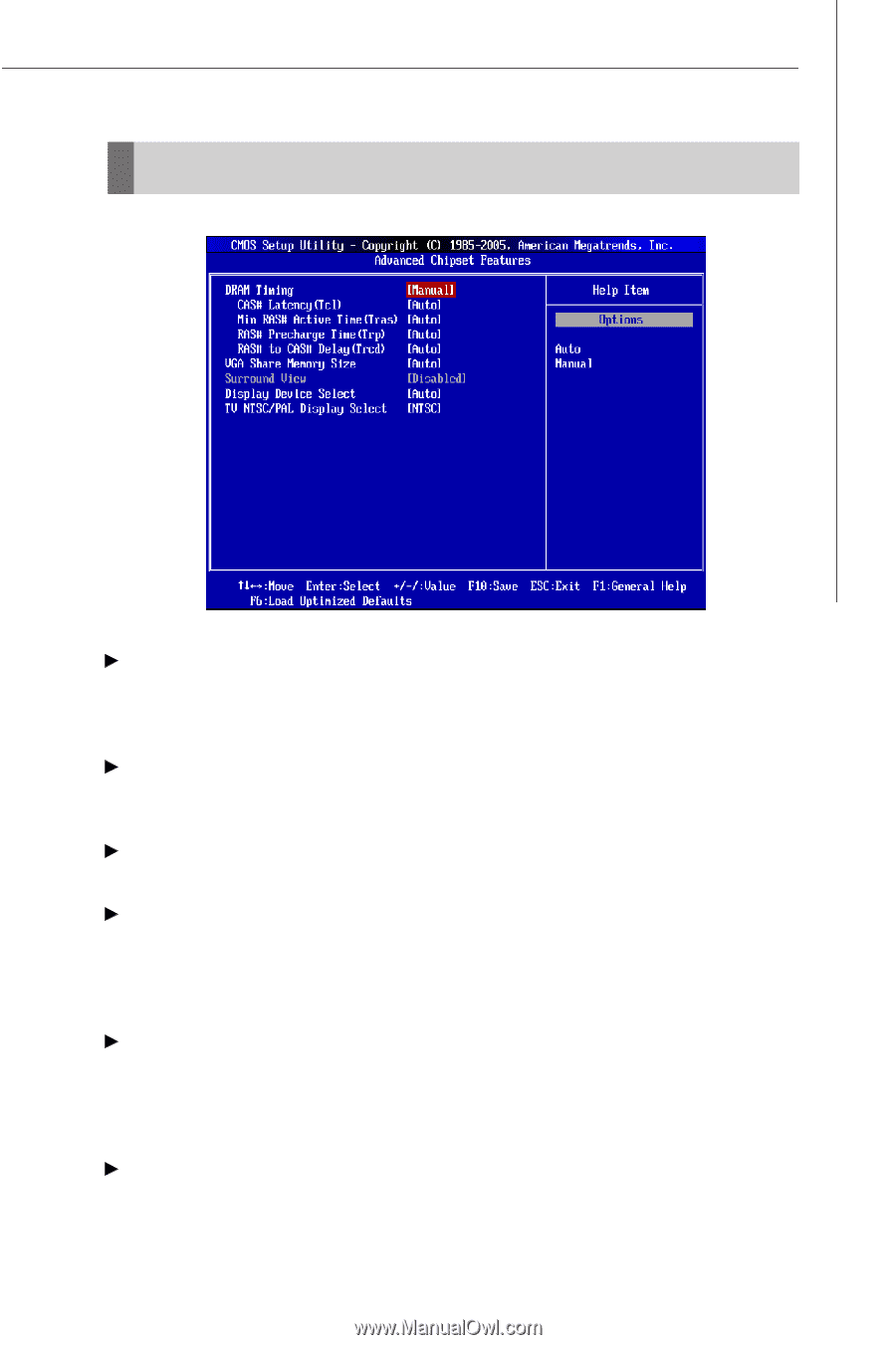
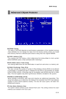
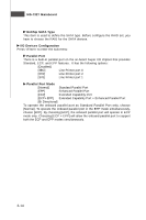
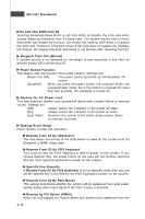
Advanced Chipset Features BIOS Setup DRAM Timing The value in this field depends on performance parameters of the installed memory chips (DRAM). Do not change the value from the factory setting unless you install new memory that has a different performance rating than the original DRAMs. CAS# Latency (Tcl) This controls the CAS latency, which determines the timing delay (in clock cycles) before SDRAM starts a read command after receiving it. M in RAS# Active Time (Tras) This setting determines the time RAS takes to read from and write to a memory cell. RAS# Precharge Time (Trp) This item controls the number of cycles for Row Address Strobe (RAS) to be allowed to precharge. If insufficient time is allowed for the RAS to accumulate its charge before DRAM refresh, refreshing may be incomplete and DRAM may fail to retain data. This item applies only when synchronous DRAM is installed in the system. RAS# to CAS# Delay (Trcd) W hen DRAM is refreshed, both rows and columns are addressed separately. This setup item allows you to determine the timing of the transition from RAS (row address strobe) to CAS (column address strobe). The less the clock cycles, the faster the DRAM performance. VGA Share Memory Size The system shares memory to the onboard VGA card. This setting controls the exact memory size shared to the VGA card. 3-11
-
 1
1 -
2
-
3
-
4
-
5
-
6
-
7
-
8
-
9
-
10
-
11
-
12
-
13
-
14
-
15
-
16
-
17
-
18
-
19
-
20
-
21
-
22
-
23
-
24
-
25
-
26
-
27
-
28
-
29
-
30
-
31
-
32
-
33
-
34
-
35
-
36
-
37
-
38
-
39
-
40
-
41
-
 42
42 -
 43
43 -
 44
44 -
 45
45 -
 46
46 -
 47
47 -
 48
48 -
 49
49 -
 50
50 -
 51
51 -
 52
52 -
53
-
54
-
55
-
56
-
57
-
58
-
59
-
60
-
61
-
62
-
63
-
64
-
65
-
66
-
67
-
68
-
69
-
70
-
71
-
72
-
73
-
74
-
75
-
76
-
77
-
78
-
79
-
80
-
81
-
82
-
83
-
84
-
85
-
86
-
87
-
88
-
89
 |
 |