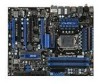
MSI P55 GD80 User Guide - Page 72
CH1/ CH2 CAS Latency CL
 |
UPC - 816909062380
View all MSI P55 GD80 manuals
Add to My Manuals
Save this manual to your list of manuals |
Page 72 highlights
▍ BIOS Setup ▶ DRAM Timing Mode Select whether DRAM timing is controlled by the SPD (Serial Presence Detect) EEPROM on the DRAM module. Setting to [Auto] enables DRAM timings and the following "Advance DRAM Configuration" sub-menu to be determined by BIOS based on the configurations on the SPD. Selecting [Manual] allows users to configure the DRAM timings and the following related "Advance DRAM Configuration" sub-menu manually. ▶ Advance DRAM Configuration When the DRAM Timing Mode is set to [Manual], this sub-menu will available. Press to enter the sub-menu. ▶ CH1/ CH2 1T/2T Memory Timing This item controls the SDRAM command rate. Select [1N] makes SDRAM signal controller to run at 1N (N=clock cycles) rate. Selecting [2N] makes SDRAM signal controller run at 2N rate. ▶ CH1/ CH2 CAS Latency (CL) This controls the CAS latency, which determines the timing delay (in clock cycles) before SDRAM starts a read command after receiving it. ▶ CH1/ CH2 tRCD When DRAM is refreshed, both rows and columns are addressed separately. This setup item allows you to determine the timing of the transition from RAS (row address strobe) to CAS (column address strobe). The less the clock cycles, the faster the DRAM performance. ▶ CH1/ CH2 tRP This setting controls the number of cycles for Row Address Strobe (RAS) to be allowed to precharge. If insufficient time is allowed for the RAS to accumulate its charge before DRAM refresh, refresh may be incomplete and DRAM may fail to retain data. This item applies only when synchronous DRAM is installed in the system. ▶ CH1/ CH2 tRAS This setting determines the time RAS takes to read from and write to memory cell. ▶ CH1/ CH2 tRFC This setting determines the time RFC takes to read from and write to a memory cell. ▶ CH1/ CH2 tWR Minimum time interval between end of write data burst and the start of a precharge command. Allows sense amplifiers to restore data to cells. ▶ CH1/ CH2 tWTR Minimum time interval between the end of write data burst and the start of a column-read command. It allows I/O gating to overdrive sense amplifiers before read command starts. ▶ CH1/ CH2 tRRD Specifies the active-to-active delay of different banks. 3-24
-
 1
1 -
2
-
3
-
4
-
5
-
6
-
7
-
8
-
9
-
10
-
11
-
12
-
13
-
14
-
15
-
16
-
17
-
18
-
19
-
20
-
21
-
22
-
23
-
24
-
25
-
26
-
27
-
28
-
29
-
30
-
31
-
32
-
33
-
34
-
35
-
36
-
37
-
38
-
39
-
40
-
41
-
42
-
43
-
44
-
45
-
46
-
47
-
48
-
49
-
50
-
51
-
52
-
53
-
54
-
55
-
56
-
57
-
58
-
59
-
60
-
61
-
62
-
63
-
64
-
65
-
66
-
 67
67 -
 68
68 -
 69
69 -
 70
70 -
 71
71 -
 72
72 -
 73
73 -
 74
74 -
 75
75 -
 76
76 -
 77
77 -
78
-
79
-
80
-
81
-
82
-
83
-
84
-
85
-
86
-
87
-
88
-
89
-
90
-
91
-
92
-
93
-
94
-
95
-
96
-
97
-
98
-
99
-
100
-
101
-
102
-
103
-
104
-
105
-
106
-
107
-
108
-
109
-
110
-
111
-
112
-
113
-
114
-
115
-
116
-
117
-
118
-
119
-
120
-
121
-
122
-
123
-
124
-
125
-
126
-
127
-
128
-
129
-
130
-
131
-
132
-
133
-
134
-
135
-
136
-
137
-
138
-
139
-
140
-
141
-
142
-
143
-
144
-
145
-
146
-
147
-
148
-
149
-
150
 |
 |
