Oki ML490 Maintenance Manual - Page 21
Temperature compensation See 2.1.8 Alarm Circuit.
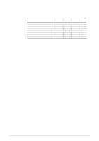
 |
View all Oki ML490 manuals
Add to My Manuals
Save this manual to your list of manuals |
Page 21 highlights
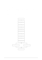
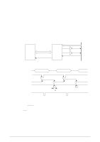
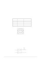
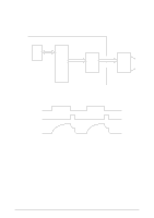
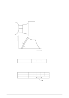
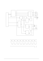
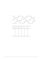
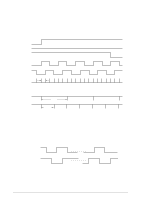
Print Compensation Control The print compensation can be made as shown below: (a) Voltage compensation (See 2.1.8 "Alarm Circuit.") (b) Temperature compensation (See 2.1.8 "Alarm Circuit.") (c) Pin stroke compensation Platen Pin 1~4 5~20 21~24 Print Head As shown in the drawing left, the stroke length up to the platen is different for each pin. Pin coil current Pin 1~4, 21~24 Pin 5~20 Time (d) Simultaneous Compensation of the number of impact pins The LSI is provided with the compensation table for each pin to make necessary compensation. Number of impact pins Few Drive time Short Many Long (e) Print mode compensation According to the thickness of the printing medium, the print mode is compensated as shown in the table below: Head Gap Range Print speed Drive time 1 2 100% 90% Short 3 85% 4 5 85% 70% Long (Drive time lengthens at each step.) 42114101 Rev.1 21 /
-
 1
1 -
2
-
3
-
4
-
5
-
6
-
7
-
8
-
9
-
10
-
11
-
12
-
13
-
14
-
15
-
 16
16 -
 17
17 -
 18
18 -
 19
19 -
 20
20 -
 21
21 -
 22
22 -
 23
23 -
 24
24 -
 25
25 -
 26
26 -
27
-
28
-
29
-
30
-
31
-
32
-
33
-
34
-
35
-
36
-
37
-
38
-
39
-
40
-
41
-
42
-
43
-
44
-
45
-
46
-
47
-
48
-
49
-
50
-
51
-
52
-
53
-
54
-
55
-
56
-
57
-
58
-
59
-
60
-
61
-
62
-
63
-
64
-
65
-
66
-
67
-
68
-
69
-
70
-
71
-
72
-
73
-
74
-
75
-
76
-
77
-
78
-
79
-
80
-
81
-
82
-
83
-
84
-
85
-
86
-
87
-
88
-
89
-
90
-
91
-
92
-
93
-
94
-
95
-
96
-
97
-
98
-
99
-
100
-
101
-
102
-
103
-
104
-
105
-
106
-
107
-
108
-
109
-
110
-
111
-
112
-
113
-
114
-
115
-
116
-
117
-
118
-
119
-
120
-
121
-
122
-
123
-
124
-
125
-
126
-
127
-
128
-
129
-
130
-
131
-
132
-
133
-
134
-
135
 |
 |
