Pioneer DEH-P900R Service Manual - Page 78
Pin Functions UPD63710GC
 |
View all Pioneer DEH-P900R manuals
Add to My Manuals
Save this manual to your list of manuals |
Page 78 highlights
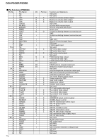
DEH-P900R,P9050 - Pin Functions (UPD63710GC) Pin No. Pin Name I/O 1 GND 2 HOLD I/O 3 MIRR I/O 4 FOK O 5 rst I 6 A0 I 7 stb I 8 sck I 9 SO O 10 SI I 11 VDD 12 DA.VDD 13 NC 14, 15 DA.GND 16 NC 17 DA.VDD 18 R+ O 19 R- O 20 L- O 21 L+ O 22 X.VDD 23 xtal O 24 XTAL I 25 X.GND 26 VDD 27 EMPH O 28 FLAG O 29 DIN I 30 DOUT O 31 SCKIN I 32 SCKO O 33 LRCKIN I 34 LRCK O 35 WDCK O 36 TX O 37 GND 38 C16M O 39 LIMIT I 40 VDD 41 LOCK O 42 RFCK O 43 WFCK O 44 PLCK O 45 GND 46 C1D1 O 47 C1D2 O 48 C2D1 O 49 C2D2 O 50 C2D3 O 51 VDD 52 PACK O 53 TSO O 54 TSI I 55 tsck I 56 TSTB I 57 GND 58 TEST I Function and Operation Logic circuit GND Defect detection output MIRR output RFOK signal output Reset signal input Command/parameter identification signal input Data strobe signal input Clock signal input for serial data input/output Serial data and status signal output Serial data input Positive power supply terminal to logic circuit Positive power supply terminal to D/A converter Not used D/A converter GND Not used Positive power supply terminal to D/A converter Right channel audio data output Right channel audio data output Left channel audio data output Left channel audio data output Positive power supply terminal to crystal oscillation circuit Crystal oscillator connect pin Crystal oscillator connect pin Crystal oscillation circuit GND Positive power supply terminal to logic circuit Output pin for the pre-emphasis data in the sub-Q code Flag output pin to indicate that audio data currently being output consists of noncorrectable data Serial data input to internal DAC Serial audio data output Serial clock input to internal DAC Audio data that is output from DOUT changes at rising edge of this clock LRCK signal input to internal DAC Signals to distinguish the right and left channels of the audio data output from DOUT Output double the frequency of LRCK Digital audio interface data output Logic circuit GND Oscillator clock buffering output Status of the pin is output at Bit 5 of the status output Positive power supply terminal to logic circuit EFM synchronous detection signal Frame synchronous signal of XTAL-system Frame synchronous signal of PLL-system Monitor pin of bit clock Logic circuit GND Output pin for indicating the C1 error correction results Output pin for indicating the C1 error correction results Output pin for indicating the C2 error correction results Output pin for indicating the C2 error correction results Output pin for indicating the C2 error correction results Positive power supply terminal to logic circuit CD-TEXT PACK synchronous signal CD-TEXT data serial output CD-TEXT control parameter serial input CD-TEXT serial clock input CD-TEXT parameter strobe signal input Logic circuit GND Test pin 78
-
 1
1 -
2
-
3
-
4
-
5
-
6
-
7
-
8
-
9
-
10
-
11
-
12
-
13
-
14
-
15
-
16
-
17
-
18
-
19
-
20
-
21
-
22
-
23
-
24
-
25
-
26
-
27
-
28
-
29
-
30
-
31
-
32
-
33
-
34
-
35
-
36
-
37
-
38
-
39
-
40
-
41
-
42
-
43
-
44
-
45
-
46
-
47
-
48
-
49
-
50
-
51
-
52
-
53
-
54
-
55
-
56
-
57
-
58
-
59
-
60
-
61
-
62
-
63
-
64
-
65
-
66
-
67
-
68
-
69
-
70
-
71
-
72
-
 73
73 -
 74
74 -
 75
75 -
 76
76 -
 77
77 -
 78
78 -
 79
79 -
 80
80 -
 81
81 -
 82
82 -
 83
83 -
84
-
85
-
86
-
87
-
88
-
89
 |
 |
