Pioneer PDP-503CMX Technical Manual - Page 14
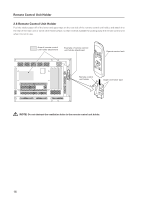
Controls and Connectors, 4 Pin layout
 |
View all Pioneer PDP-503CMX manuals
Add to My Manuals
Save this manual to your list of manuals |
Page 14 highlights
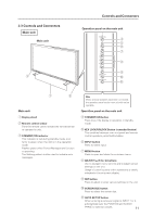
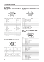
Controls and Connectors 2.4 Pin layout INPUT 1 (Mini D-sub, 15-pin connector; female) pin layout 5 1 RS-232C terminal (D-sub 9-pin connector; male) pin layout 1 5 10 6 15 11 Pin No. $ INPUT1 input terminals 1 R or CR/PR 2 G or Y 3 B or CB/PB 4 NC (not connected) 5 GND 6 GND 7 GND 8 GND 9 DDC +5V 10 GND 11 NC (not connected) 12 DDC SDA 13 HD or H/V SYNC 14 VD 15 DDC SCL % INPUT1 output terminals NC (not connected) NC (not connected) NC (not connected) Combination IN/OUT terminal pin layout 6 5 4 3 2 1 Pin No. Combination IN 1 GND 2 NC (not connected) 3 TxD (output) 4 NC (not connected) 5 RxD (input) 6 NC (not connected) Combination OUT GND NC (not connected) RxD (input) NC (not connected) TxD (output) NC (not connected) 14 6 9 Pin No. 1 2 3 4 5 6 7 8 9 Signal NC (not connected) TxD (Transmit Data) RxD (Receive Data) NC (not connected) GND NC (not connected) NC (not connected) RTS (Request To Send) NC (not connected) INPUT 5 # (DVI-D 24 pin connector; female) pin layout 1 2 Pin No. 9 17 24 16 Signal Assignment 1 T.M.D.S. Data2- 2 T.M.D.S. Data2+ 3 T.M.D.S. Data2/4 Shield 4 NC (No connection) 5 NC (No connection) 6 DDC Clock 7 DDC Data 8 NC (No connection) 9 T.M.D.S. Data1- 10 T.M.D.S. Data1+ 11 T.M.D.S. Data1/3 Shield 12 NC (No connection) 13 NC (No connection) 14 +5V Power 15 GND 16 Hot Plug Detect 17 T.M.D.S. Data0 - 18 T.M.D.S. Data0+ 19 T.M.D.S. Data0/5 Shield 20 NC (No connection) 21 NC (No connection) 22 T.M.D.S. Clock Shield 23 T.M.D.S. Clock+ 24 T.M.D.S. Clock-
-
 1
1 -
2
-
3
-
4
-
5
-
6
-
7
-
8
-
 9
9 -
 10
10 -
 11
11 -
 12
12 -
 13
13 -
 14
14 -
 15
15 -
 16
16 -
 17
17 -
 18
18 -
 19
19 -
20
-
21
-
22
-
23
-
24
-
25
 |
 |
