Pioneer VSX-07TX Service Manual - Page 68
Pioneer VSX-07TX Manual
 |
View all Pioneer VSX-07TX manuals
Add to My Manuals
Save this manual to your list of manuals |
Page 68 highlights
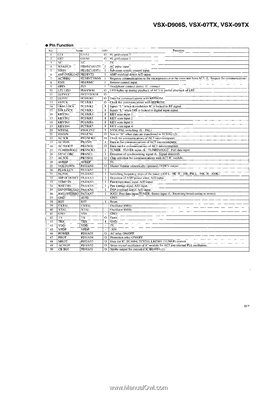
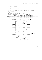
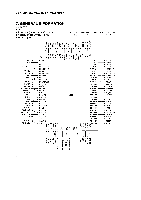
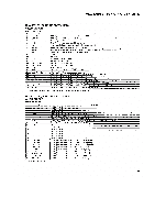
VSX-D906S, VSX-07TX, VSX-09TX • Pin Function No. Name I/O Function I GIl GI/A1 0 FL grid output 2. 2 G12 GO/A0 0 FL grid output 1. 3 NC NC 5V, 4 WAKEUP PEO/ECO/INTO I AC pulse input. 5 MRIN PE1/EC I/INT I I Sub room remote control input. 6 AMP OVERLOAD PE2/INT2 I AMP overload detect A/D input. 7 AC3REQ PE3/INT3/NMI I Requests communications to the microprocessor in the main unit from AC3. (L: Request for conununication) 8 RMS PE4/RMC I Remote control input. 9 HPIN PE5 I Headphone connect detect. H :connect 10 LFE LED PE6/PWM 0 LED lights up during playback of AC3 or partial playback of LEE 11 EEPVCC PE7/TO/ADJ 0 12 EEPDT PCO/KRO 0 Data for communications with EEPROM. 13 EEPCK PC1/KRI 0 Clock for communications with EEPROM. 14 DEM.LOCK PC2/KR2 I Inputs "L" when demodulator IC is locked to RF signal. 15 DIR.LOCK PC3/KR3 I Inputs "L" when DIR is locked to digital input signal. 16 KEYINI PC4/KR4 1 KEY scan input 1. 17 KEYIN2 PC5/KR5 I KEY scan input 2. 18 KEYIN3 PC&KR6 l KEY scan input 3. 19 KEYIN4 PC7/KR7 l KEY scan input 4. 20 NT/PAL PBO/CINT I NTSC/PAL switching. (L : PAL) 21 91620N PB1/CSO 0 Sets to "H" when data are transferred to TC9162 (2). 22 AC3CK PB2/SCKO 0 Clock for communications of AC3 microcomputer. 23 AC3DIN PB3/SIO I Data in for communications of AC3 microcomputer. 24 AC3DOUT P134/S00 0 Data out for communications of AC3 microcomputer. 25 TUNED/JOG2 PB5/SCK I I TUNER TUNER input. (L ! TUNED)/J0G2 : Port data input 26 SYNC.DEC PB6/SC I I Detection of synchronizing signal (L: Simla] detected) 27 AC3CE PB7/S01 0 Chip selection for communications with AC3 IC module. 28 AVREF AVREF - 5V. 29 VOLDOWN PAO/ANO 0 Master Volume (electrically operated) DOWN output. 30 PEAK.LEV PA I /AN I I 31 9IQIOK PA2/AN2 I Switching frequency steps of the tuner. (AM L : 9K II : 10K, FM L : 50K ft 100K) 32 AMP DC DETECT PA3/AN3 1 Detection of AMP power error, A/D input. 33 TEMP-IN PA4/AN4 I Fan temperature input. AID input. 34 WATT-IN PA5/AN5 1 Fan wattage input. A/D input. 35 DSP OVERLOAD PA6/AN6 I DSP overload detect. A/D input. 36 JOG 1/STEREO PA7/AN7 I JOG I : Port data input/TUNER: Stereo input (L: Receiving broadcasting in stereo). 37 GND AVSS GND. 38 RST RST I Reset. 39 EXTAL EXTAL - Oscillator 8MHz. 40 XTAL XTAL Oscillator 8MHz. 41 GND VSS - GND. 42 TX TX 0 Open. 43 TEX TEX I GND. 44 VDD VDD 5V. 45 VFDP VFDP -30V. 46 POWER PDO/A55 0 AC relay ON/OFF. 47 PROT PD1/A54 0 Protection relay ON/OFF. 48 MRDT PD2/A53 0 Data for IC. BU4094, TC9210, LM7001 (TUNER) control. 49 AC3STP PD3/A52 0 Stops crystal oscillation of IC module for AC3 and internal PLL oscillation. 50 CE BUI PD4/A51 0 Strobe output for extended IC BU4094 (1). 97
-
 1
1 -
2
-
3
-
4
-
5
-
6
-
7
-
8
-
9
-
10
-
11
-
12
-
13
-
14
-
15
-
16
-
17
-
18
-
19
-
20
-
21
-
22
-
23
-
24
-
25
-
26
-
27
-
28
-
29
-
30
-
31
-
32
-
33
-
34
-
35
-
36
-
37
-
38
-
39
-
40
-
41
-
42
-
43
-
44
-
45
-
46
-
47
-
48
-
49
-
50
-
51
-
52
-
53
-
54
-
55
-
56
-
57
-
58
-
59
-
60
-
61
-
62
-
 63
63 -
 64
64 -
 65
65 -
 66
66 -
 67
67 -
 68
68 -
 69
69 -
 70
70 -
 71
71 -
 72
72 -
 73
73 -
74
-
75
-
76
-
77
-
78
-
79
-
80
-
81
-
82
-
83
-
84
 |
 |