Pioneer VSX-52TX Service Manual - Page 135
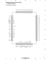
AK4628VQE DSP ASSY: IC701, Pin Function
 |
View all Pioneer VSX-52TX manuals
Add to My Manuals
Save this manual to your list of manuals |
Page 135 highlights
5 6 7 AK4628VQE (DSP ASSY: IC701) • 8 ch Codec Pin Function No. Pin Name 1 SDOS 2 I2C 3 SMUTE 4 BICK 5 LRCK 6 SDTI1 7 SDTI2 8 SDTI3 9 SDTO 10 DAUX 11 DFSO 12 SDTI4 13 DZFE 14 TVDD 15 DVDD 16 DVSS 17 PDN 18 TST1 19 CAD1 20 CAD0 21 LOUT4 22 ROUT4 23 LOUT3 24 ROUT3 25 LOUT2 26 ROUT2 27 LOUT1 28 ROUT1 29 TST2 30 NC 31 LIN 32 RIN 33 DZF2/OVF 34 VCOM 35 VREFH 36 AVDD 37 AVSS 38 DZF1 39 MCLK 40 P/S 41 CSN 42 CCLK 43 CDTI 44 TDMO I/O Pin Function I SDTO source selection I Serial control mode selection I Soft mute I Audio serial data clock I Input channel clock I DAC1 audio serial data input I DAC2 audio serial data input I DAC3 audio serial data input O Audio serial data output I Auxiliary audio serial data input I Double-speed sampling mode I DAC4 audio serial data input I Zero-input detecting function validity pin − Power supply for output buffer − Digital power supply − Digital ground I Power down and reset I Test pin I Chip address 1 pin I Chip address 0 pin O Analog output of DAC 4 L channnel O Analog output of DAC 4 R channnel O Analog output of DAC 3 L channnel O Analog output of DAC 3 R channnel O Analog output of DAC 2 L channnel O Analog output of DAC 2 R channnel O Analog output of DAC 1 L channnel O Analog output of DAC 1 R channnel − No connect − No connect I L chnnel analog input I R chnnel analog input O Zero input detection 2 / Overflow detection of analog input O Common voltage output I Reference voltage input − Analog power supply − Analog ground O Zero input detection 1 I Master clock input I Parallel/serial input I Chip select I Control data clock I Control data input I TDM I/F format mode VSX-52TX 5 6 7 8 A Active B L C D H H L E F 135 8
-
 1
1 -
2
-
3
-
4
-
5
-
6
-
7
-
8
-
9
-
10
-
11
-
12
-
13
-
14
-
15
-
16
-
17
-
18
-
19
-
20
-
21
-
22
-
23
-
24
-
25
-
26
-
27
-
28
-
29
-
30
-
31
-
32
-
33
-
34
-
35
-
36
-
37
-
38
-
39
-
40
-
41
-
42
-
43
-
44
-
45
-
46
-
47
-
48
-
49
-
50
-
51
-
52
-
53
-
54
-
55
-
56
-
57
-
58
-
59
-
60
-
61
-
62
-
63
-
64
-
65
-
66
-
67
-
68
-
69
-
70
-
71
-
72
-
73
-
74
-
75
-
76
-
77
-
78
-
79
-
80
-
81
-
82
-
83
-
84
-
85
-
86
-
87
-
88
-
89
-
90
-
91
-
92
-
93
-
94
-
95
-
96
-
97
-
98
-
99
-
100
-
101
-
102
-
103
-
104
-
105
-
106
-
107
-
108
-
109
-
110
-
111
-
112
-
113
-
114
-
115
-
116
-
117
-
118
-
119
-
120
-
121
-
122
-
123
-
124
-
125
-
126
-
127
-
128
-
129
-
 130
130 -
 131
131 -
 132
132 -
 133
133 -
 134
134 -
 135
135 -
 136
136 -
 137
137 -
 138
138 -
 139
139 -
 140
140 -
141
-
142
-
143
-
144
-
145
-
146
-
147
-
148
-
149
 |
 |
