Pioneer VSX-52TX Service Manual - Page 137
Pin Function
 |
View all Pioneer VSX-52TX manuals
Add to My Manuals
Save this manual to your list of manuals |
Page 137 highlights
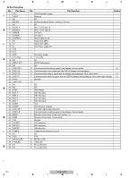
5 Pin Function No. Pin Name 1 12VTRIGGER 2 DISP RST 3 DISP EN 4 DISP RDY 5 OSD/DISP DI 6 DISP DO 7 OSD/DISP CLK 8 GND 9 CNVSS 10 - 11 - 12 XRESET 13 XOUT 14 GND 15 XIN 16 5V 17 NMI 18 WAKEUP 19 1394 INT 20 1W WUP 21 DECO MUTE 22 DSP OL 23 DC PROT 24 Boad DET 25 MIC DET 26 1394 RST 27 1394 CS 28 1394 CK 29 1394 DO 30 1394 DI 31 232C RXD 32 232C TXD 33 CLK 34 232C CTS 35 DSP DI 36 DSP DO 37 DSP CLK 38 DSP RST 39 DSP SS 40 BUSY 41 DSP HREQ 42 DSP MODE 43 DSP MUTE 44 ADMD 45 DIR DO 46 DIR CS 47 LSSN 48 DIR RST 49 DIR ERR 50 XTLO 6 7 8 I/O Pin Function Active O "H" at ON O Display microcomputer reset signal L: reset, H: release reset (pulldown) A O Communication enabling signal to the display microcomputer H I Communication enabling signal from the display microcomputer H O Communication data out signal with the OSD-IC/display microcomputer (N ch open drain: pullup) I Communication data in signal with the display microcomputer (N ch open drain) O Communication clock signal with the OSD-IC/display microcomputer − Ground − 5.1kΩ pulldown O L" fixed O L" fixed − Reset B − Oscillator − Ground − Oscillator − 5V power supply I Cannot use it as usual input port (100kΩ pullup) I Wakeup H I INT for 1394 (Not used) Standby with the circuit. I Wakeup signal at standby (from the display microcomputer) (pulldown) H I Boot success detecting port of 1st DSP O Communication enabling signal to the display microcomputer H O OSD-IC reset signal L: reset, H: release reset C O OSD-IC chip select signal H O At data transfer to the OSD-IC: "H" O Reset for 1394 "L" fixed. O Standby for 1394 (Not used) "L" fixed. H O CK for 1394 O DO for 1394 I DI for 1394 O For 232C rewriting (data output) I For 232C rewriting (data input) - Not used O For 232C rewriting (communication permission) D O Communication data out signal with the DSP1 microcomputer I Communication data in signal with the DSP2 microcomputer O Communication clock signal with the DSP microcomputer O DSP microcomputer reset signal L: reset, H: release reset O Slave select signal to DSP microcomputer I MCACC used L O Error detection signal of DSP microcomputer L O Mode selection of DSP microcomputer (ROM/RAM) H: ROM mode, L: RAM (PPP) mode H O DSP Assy mute H - NC E I Communication data in signal with the DIR/DAC O Communication chip select signal with the DIR/DAC - NC O DIR reset signal I Lock/Unlock signal from DIR O Selection X'tal to DIR F VSX-52TX 137 5 6 7 8
-
 1
1 -
2
-
3
-
4
-
5
-
6
-
7
-
8
-
9
-
10
-
11
-
12
-
13
-
14
-
15
-
16
-
17
-
18
-
19
-
20
-
21
-
22
-
23
-
24
-
25
-
26
-
27
-
28
-
29
-
30
-
31
-
32
-
33
-
34
-
35
-
36
-
37
-
38
-
39
-
40
-
41
-
42
-
43
-
44
-
45
-
46
-
47
-
48
-
49
-
50
-
51
-
52
-
53
-
54
-
55
-
56
-
57
-
58
-
59
-
60
-
61
-
62
-
63
-
64
-
65
-
66
-
67
-
68
-
69
-
70
-
71
-
72
-
73
-
74
-
75
-
76
-
77
-
78
-
79
-
80
-
81
-
82
-
83
-
84
-
85
-
86
-
87
-
88
-
89
-
90
-
91
-
92
-
93
-
94
-
95
-
96
-
97
-
98
-
99
-
100
-
101
-
102
-
103
-
104
-
105
-
106
-
107
-
108
-
109
-
110
-
111
-
112
-
113
-
114
-
115
-
116
-
117
-
118
-
119
-
120
-
121
-
122
-
123
-
124
-
125
-
126
-
127
-
128
-
129
-
130
-
131
-
 132
132 -
 133
133 -
 134
134 -
 135
135 -
 136
136 -
 137
137 -
 138
138 -
 139
139 -
 140
140 -
 141
141 -
 142
142 -
143
-
144
-
145
-
146
-
147
-
148
-
149
 |
 |
