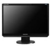
Samsung 2220WM Service Manual - Page 3
Mian Board, 2 Power Board, Circuit Descriptions, 1 Overall Block Structture, 2 IP Board Part Power - parts
 |
UPC - 729507801940
View all Samsung 2220WM manuals
Add to My Manuals
Save this manual to your list of manuals |
Page 3 highlights
9-3 Connecting the monitor ...33 9-4 Monitor Assembly ... 34 9-5 Attaching a Base ... 35 10. Disassembly and Reassembly ...36 10-1 Disassembly ...36 10-2 Assembly Block ...39 11. PCB Diagram ...40 11-1 Mian Board...40 12-2 Power Board...41 12. Circuit Descriptions ...42 12-1 Overall Block Structture ...42 12-2 IP Board Part (Power) Schematic Diagrams ...44 12-3 IP Board (Inverter) Schematic Diagrams ...45 13. Reference Information ...46 13-1 Technical Terms ...46 13-2 Pin Assignments ...48 13-3 Timing Chart ...49 3
-
 1
1 -
 2
2 -
 3
3 -
 4
4 -
 5
5 -
 6
6 -
 7
7 -
 8
8 -
 9
9 -
10
-
11
-
12
-
13
-
14
-
15
-
16
-
17
-
18
-
19
-
20
-
21
-
22
-
23
-
24
-
25
-
26
-
27
-
28
-
29
-
30
-
31
-
32
-
33
-
34
-
35
-
36
-
37
-
38
-
39
-
40
-
41
-
42
-
43
-
44
-
45
-
46
-
47
-
48
-
49
 |
 |

3
9-3 Connecting the monitor ………………………………………………………………………………………………………………………
33
9-4 Monitor Assembly ……………………………………………………………………………………………………………………………..
34
9-5 Attaching a Base ……………………………………………………………………………………………………………………………..
35
10.
Disassembly and Reassembly ……………………………………………………………………………………………………………………………
36
10-1 Disassembly ……………………………………………………………………………………………………………………………………
36
10-2 Assembly Block ………………………………………………………………………………………………………………………………..
39
11.
PCB Diagram ………………………………………………………………………………………………………………………………………………
40
11-1 Mian Board
...................................................................................................................................................................................................
40
12-2 Power Board
..................................................................................................................................................................................................
41
12.
Circuit Descriptions
......................................................................................................................................................................................................
42
12-1 Overall Block Structture
.............................................................................................................................................................................
42
12-2 IP Board Part (Power) Schematic Diagrams
...........................................................................................................................................
44
12-3 IP Board (Inverter) Schematic Diagrams ……………………………………………………………………………………………………
45
13.
Reference Information ……………………………………………………………………………………………………………………………………
46
13-1 Technical Terms ………………………………………………………………………………………………………………………………
46
13-2 Pin Assignments ………………………………………………………………………………………………………………………………
48
13-3 Timing Chart …………………………………………………………………………………………………………………………………..
49