SanDisk 4GB micro SDHC Memory Card for Product Manual - Page 15
Pins and Registers - drivers
 |
UPC - 084331428832
View all SanDisk 4GB micro SDHC Memory Card for manuals
Add to My Manuals
Save this manual to your list of manuals |
Page 15 highlights
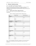
SanDisk microSD™, microSDHC™ and microSDXC™ cards 3 INTERFACE DESCRIPTION OEM Product Manual 2.5 3.1 Pins and Registers The SanDisk microSD™ Card Product Family has exposed contacts on one side. The host uses a dedicated connector to connect to microSD cards. In Table 4, pin assignments for the SanDisk microSD Card are described for SD Bus Mode and SPI Bus Mode Note: Pin assignments are provided by the SDA Physical Layer Specification, Version 3.01 and associated addendums (microSD). For more details, refer to Section 3.7 of the SDA Physical Layer Specification, Version 3.01 Table 4: SD Bus Mode Pin Assignment Pin No. SD Mode SPI mode Name Type1 Description Name Type1 Description 1 DAT22,5 I/O/PP Data Line [bit 2] RSV - Reserved 2 CD/DAT32 I/O/PP3 Card Detect/Data Line [bit 3] CS I3 Chip select (active low) 3 CMD PP Command/Response DataIn I Data In 4 VDD S Supply Voltage VDD S Supply Voltage 5 CLK I Clock SCLK I Clock 6 VSS S Supply voltage ground VSS S Supply voltage ground 7 DAT0 I/O/PP Data Line [bit 1] 8 DAT12,4 I/O/PP Data Line [bit 2] DataOUT RSV4 O/PP - Data Out Reserved Notes: 1. 2. 3. 4. 5. Type Key: S=power supply; I=input; O=output using push-pull drivers; PP=I/O using push-pull drivers. The extended DAT lines (DAT1-DAT3) are input on power up. They start to operate as DAT lines after the SET_BUS_WIDTH command. It is the responsibility of the host designer to connect external pull-up resistors to all data lines even if only DAT0 is to be used. If not, there may be unexpected high current consumption due to the floating inputs of DAT1 & DAT2 (if they are not used). At power up this line has a 50KOhm pull-up enabled in the card. This resistor serves two functions: Card Detection and Mode Selection. For Mode Selection, the host can drive the line high or let it be pulled high to select SD mode. If the host wants to select SPI mode, it should drive the line low. For Card Detection, the host detects that the line is pulled high. The user should disconnect this pull-up with SET_CLR_CARD_DETECT (ACMD42) command during regular data transfer. DAT1 line may be used as Interrupt Output (from the Card) in SDIO mode during all the times that it is not in use for data transfer operations. DAT2 line may be used as Read Wait signal in SDIO mode. January 2012 Version 2.5 © 2008 - 2012 SanDisk Corporation. SanDisk Confidential, subject to all applicable non-disclosure agreements 10
-
 1
1 -
2
-
3
-
4
-
5
-
6
-
7
-
8
-
9
-
 10
10 -
 11
11 -
 12
12 -
 13
13 -
 14
14 -
 15
15 -
 16
16 -
 17
17 -
 18
18 -
 19
19 -
 20
20 -
21
-
22
-
23
-
24
-
25
-
26
 |
 |
