SanDisk 4GB micro SDHC Memory Card for Product Manual - Page 16
Bus Topology, Hot Insertion and Power Protection, Electrical Interface
 |
UPC - 084331428832
View all SanDisk 4GB micro SDHC Memory Card for manuals
Add to My Manuals
Save this manual to your list of manuals |
Page 16 highlights
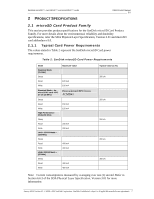
SanDisk microSD™, microSDHC™ and microSDXC™ cards OEM Product Manual 2.5 Each card has a set of information registers. Register descriptions and SDA references are provided in Section 5.0 of the SDA Physical Layer Specification, Version 3.01. Table 5: microSD Card Product Family Register Overview Register Abbreviation CID RCA CSD SCR OCR SSR CSR Width (in bits) Register Name 128 Card identification number 16 Relative card address 128 Card specific data 64 SD configuration register 32 Operation condition register 512 SD status register 32 Card status register 3.2 Bus Topology The family of SanDisk microSD products supports two communication protocols: SD and SPI. For more details, refer to Section 3.5 of the SDA Physical Layer Specification, Version 3.01. Section 6 of the specification contains a bus circuitry diagram for reference. 3.2.1 SD Bus For more details, refer to Section 3.5.1 of the SDA Physical Layer Specification, Version 3.01. 3.2.2 SPI Bus For more details, refer to Section 3.5.2 of the SDA Physical Layer Specification, Version 3.01. 3.3 Hot Insertion and Power Protection Refer to Section 6.1 and Section 6.2 of the SDA Physical Layer Specification, Version 3.01. 3.4 Electrical Interface The power scheme of SanDisk microSD products is handled locally in each card and in the bus master. Refer to Section 6.4 of the SDA Physical Layer Specification, Version 3.01. 3.4.1 Power Up Power must be applied to the VDD pin before any I/O pin is set to logic HIGH. In other words, CMD, CLK, and DAT0-3 must be at zero (0) volts when power is applied to the VDD pin. For more information, refer to Section 6.4.1 of the SDA Physical Layer Specification, Version 3.01. January 2012 Version 2.5 © 2008 - 2012 SanDisk Corporation. SanDisk Confidential, subject to all applicable non-disclosure agreements 11
-
 1
1 -
2
-
3
-
4
-
5
-
6
-
7
-
8
-
9
-
10
-
 11
11 -
 12
12 -
 13
13 -
 14
14 -
 15
15 -
 16
16 -
 17
17 -
 18
18 -
 19
19 -
 20
20 -
 21
21 -
22
-
23
-
24
-
25
-
26
 |
 |
